Processor and Chipset Intel® SHG2 DP Server Board Technical Product Specification
Intel Order Number C11343-001 Revision 1.0
16
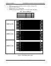
Pin Name Pin Name Pin Name
12 FD_DR1_L 24 FD_WGATE_L
2.5.1.4 Keyboard and Mouse Connectors
The PS/2-compatible keyboard and mouse connectors are mounted within a single stacked
housing. The mouse connector is stacked over the keyboard connector. External to the board,
they appear as two connectors. The keyboard controller is functionally compatible with the
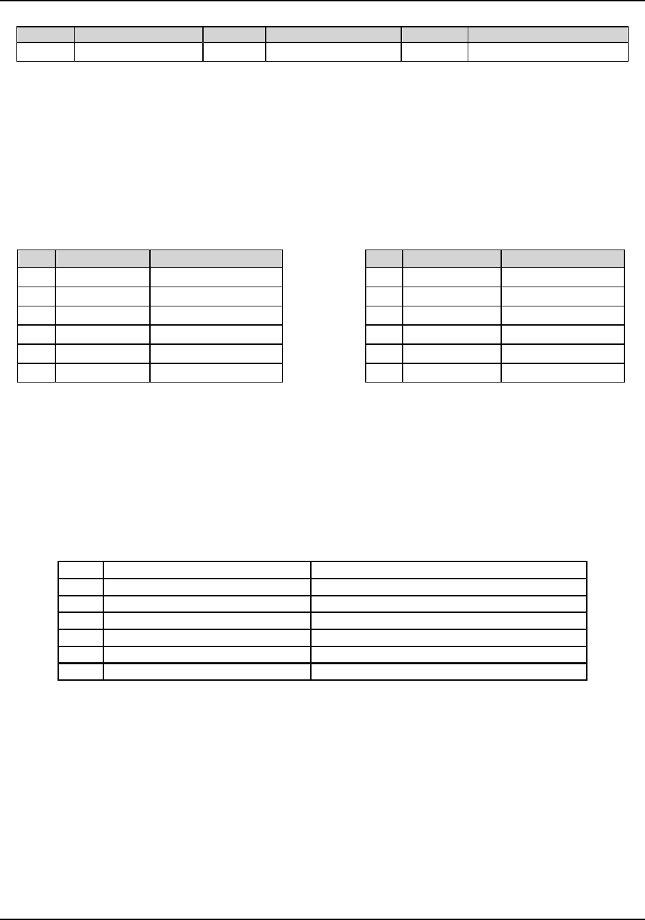
8042AH and PC87911. The keyboard and mouse connector pinouts are shown in Table 6 and
Table 7
Table 6. Keyboard Connector Pinout
Pin Signal Description
1 KEYDAT Keyboard Data
2 (NC)
3 GND Ground
4 FUSED_VCC +5 V, fused
5 KEYCLK Keyboard Clock
6 (NC)
Table 7. Mouse Connector Pinout
Pin Signal Description
1 MSEDAT Mouse Data
2 (NC)
3 GND Ground
4 FUSED_VCC +5 V, fused
5 MSECLK Mouse Clock
6 (NC)
2.5.1.5 GPIO
The PC PC87417VLA provides several of the GPIO pins that the SHG2 server board utilizes.
Table 8 identifies the pin, the signal name specified in the schematic, and a brief description of
its usage.
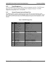
Table 8. Super I/O* GPIO Usage Table
Pin Usage Descritpion
1,2,3 PKG_SELECT<1-3> PKG ID
5 PCIXCAP1+SW To enable/disable pcix mode to slot6
49 PCIX_PME-10 Power Management Event from PCIX bus
52 PCI33_PME-10 Power Management Event from PCI bus
51 FP_PWR_LED+00 Front Panel LED control
50 PCI66_PME-10 Power Management Event from PCI 66bus
2.5.1.6 Real-time Clock
The PC97417VLA contains a DS1287, MC146818, and PC87911-compatible RTC with external
battery backup. The device also contains 242 bytes of general purpose battery-backed CMOS
RAM.
2.5.1.7 Power Management Controller
The PC87417VLA contains functionality that allows various events to control the power state of
the system (power-up or power-down). This functionality can be controlled from PCI power


