General Specifications Intel® SHG2 DP Server Board Technical Product Specification
Intel Order Number C11343-001 Revision 1.0
74
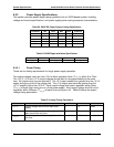
9.3.2 Power Supply Specifications
This section provides power supply design guidelines for an SHG2-based system, including
voltage and current specifications, and power supply power cycling sequence characteristics.
Table 63. SHG2 DC Power Supply Voltage Specification
Parameter Min Nom Max Units Tolerance
+3.3 V +3.168 +3.30 +3.46 V
rms
+5/-4%
+5 V +4.80 +5.00 +5.25 V
rms
+5/-4%
+12 V +11.52 +12.00 +12.60 V
rms
+5/-4%
-12 V -11.40 -12.20 -13.08 V
rms
+9/-5%
+5 VSB +4.85 +5.00 +5.25 V
rms
+5/-3%
Table 64. SHG2 Ripple and Noise Specification
+3.3V
+5V
+12V
-12V
+5VSB
50mVp-p 50mVp-p 120mVp-p 120mVp-p 50mVp-p
9.3.2.1 Power Timing
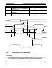
These are the timing requirements for single power supply operation.
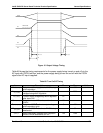
The output voltages must rise from 10% to within regulation limits (T
vout_rise
) within 5 to 70ms.
The +3.3 V, +5 V and +12 V output voltages should start to rise approximately at the same
time. All outputs must rise monotonically. The +5 V output needs to be greater than the +3.3 V
output during any point of the voltage rise. The +5 V output must never be greater than the
+3.3 V output by more than 2.25 V. Each output voltage shall reach regulation within 50ms
(T
vout_on
) of each other during turn on of the power supply. Each output voltage shall fall out of
regulation within 400msec (T
vout_off
) of each other during turn off. Table 65 shows the output
voltage timing parameters.
Table 65. Voltage Timing Parameters
Item Description Min Max Units
T
vout_rise
Output voltage rise time from each main
output.
5 70 msec
T
vout_on
All main outputs must be within regulation of
each other within this time.
50 msec
T
vout_off
All main outputs must leave regulation within
this time.
400 msec


