Intel® SHG2 DP Server Board Technical Product Specification Clock Generation and Distribution
Revision 1.0 Intel Order Number C11343-001
27
4. Clock Generation and Distribution
All buses on the Intel SHG2 server board operate using synchronous clocks. Clock
synthesizer/driver circuitry on the baseboard generates clock frequencies and voltage levels as
required, including the following:
•
100 MHz at 2.5 V logic levels - for CPU1 and CPU2, the CMIC-LE, memory buffer, and
the ITP port.
•
48 MHz at 3.3V logic levels – for CSB5 and Super I/O.
•
33.3 MHz at 3.3 V logic levels – for reference clock for the PCI bus clock driver.
Other clock sources on the Intel SHG2 server board generates:
•
66/133 MHz at 3.3V logic levels – for PCI-X Slot #6 and Ultra 160 SCSI.
•
100 MHz at 3.3V logic levels – DDR DIMMs, PCI-X Slot #1, #2 and Gigabit 82544GC.
•
40 MHz XTAL - for 7899 SCSI Controller.
•
40 MHz XTAL - for BMC.
•
32.768 XTAL - for Super I/O.
•
32.768 MHz - for BMC.
•
25 MHz XTAL - for NIC 82550PM.
•
14.318 XTAL - for main clock generator.
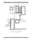
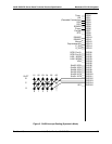
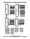
Figure 6 illustrates clock generation and distribution on the SHG2 baseboard.


