HighWire HW400c/2 User Reference Guide Rev 1.0
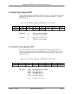
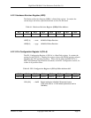
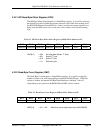
4.2.23 Write Byte Count Register (WBC)
The Write Byte Count Register is a Read/Write register. It is used for setting the
number of bytes to be written when writing to the BCM5388 SPI port.
All bytes in a given register must be written; for example, if the register to be written
itten, contains 3 bytes, then WBC[3:0] must be set to 0011. When this register is wr
the internal SPI Write State Machine is initiated. After all bytes are written to the
BCM5388 register, the WBC value is cleared.
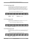
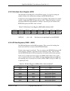
Table 53. Write Byte Count Register (WBC) Offset Address 0x1E
Bit 7 Bit 6 Bit 5 Bit 4 Bit 3 Bit 2 Bit 1 Bit 0
Reserved Reserved Reserved Reserved WBC3 WBC2 WBC1 WBC0
WBC[3:0] 1 – 0x BCM5388
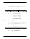
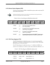
4.2.24 SPI Data egisters (S – S
ta Registers ar ding data
ytes to be read from or w
ritten values ot be uring an SPI
rite operation. Similarly, read values are not affected by writes. They are read
om the BCM5388 after an SPI read operation, and remain until the next operation.
r write, only SDR0 (offset 0x20) is used. In the
case of a multi-byte read or write, SDR0 is the least significant data byte (LSB) and
e remaining one to seven bytes are written to SDR1- SDR7 (last byte is MSB - up
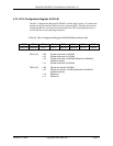
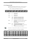
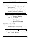
Table 54. SPI Data Registers (SDRn) Offset Address 0x20-0x27
Regis
= 0x 8 Write from one to eight bytes from the
R DR0 DR7)
The SPI Da e Read/Write registers. They are used for hol
ritten to the BCM5388 SPI port. b
W cann read back. They are written to the BCM5388 d
w
fr
In the case of a single-byte read o
th
to eight bytes total).
ter Offset Byte
SDR0 0x20 LSB
S (2-byte DR1 0x21 MSB register)
S ter) DR2 0x22 MSB (3-byte regis
SDR3 0x23 MSB (4-byte register)
SDR4 0x24 MSB (5-byte register)
SDR5 0x25 MSB (6-byte register)
SDR6 0x26 MSB (7-byte register)
SDR7 0x27 MSB (8-byte register)
October 10, 2006 Copyright 2006, SBE, Inc. Page 60


