


uPSD3212A, uPSD3212C, uPSD3212CV
120/163
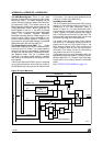
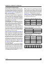
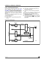
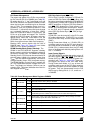
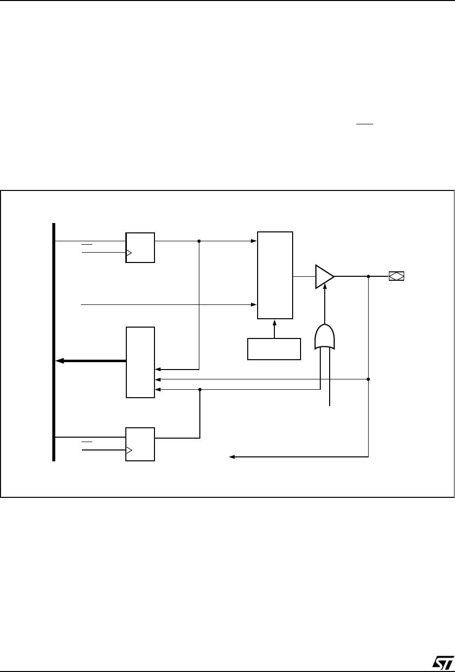
Port D – Functionality and Structure
Port D has two I/O pins (only one pin, PD1, in the
52-pin package). See Figure 63 and Figure
64., page 121. This port does not support Address
Out Mode, and therefore no Control Register is re-
quired. Of the eight bits in the Port D registers,
only Bits 2 and 1 are used to configure pins PD2
and PD1.
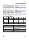
Port D can be configured to perform one or more
of the following functions:
■ MCU I/O Mode
■ CPLD Output – External Chip Select (ECS1-
ECS2)
■ CPLD Input – direct input to the CPLD, no
Input Macrocells (IMC)
■ Slew rate – pins can be set up for fast slew
rate
Port D pins can be configured in PSDsoft Express
as input pins for other dedicated functions:
■ CLKIN (PD1) as input to the macrocells flip-
flops and APD counter
■ PSD Chip Select Input (CSI, PD2). Driving this
signal High disables the Flash memory, SRAM
and CSIOP.
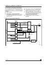
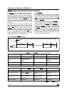
Figure 63. Port D Structure
MCU DATA BUS
DATA OUT
REG.
DQ
DQ
WR
WR
ECS
[
2:1
]
READ MUX
P
D
B
CPLD-INPUT
DIR REG.
DATA IN
ENABLE PRODUCT
TERM (.OE)
OUTPUT
SELECT
OUTPUT
MUX
PORT D PIN
DATA OUT
AI06606