


13/163
uPSD3212A, uPSD3212C, uPSD3212CV
ARCHITECTURE OVERVIEW
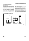
Memory Organization
The uPSD321x Devices’s standard 8032 Core has
separate 64KB address spaces for Program mem-
ory and Data Memory. Program memory is where
the 8032 executes instructions from. Data memory
is used to hold data variables. Flash memory can
be mapped in either program or data space. The
Flash memory consists of two flash memory
blocks: the main Flash (512Kbit) and the Second-
ary Flash (128Kbit). Except during flash memory
programming or update, Flash memory can only
be read, not written to. A Page Register is used to
access memory beyond the 64K bytes address
space. Refer to the PSD Module for details on
mapping of the Flash memory.
The 8032 core has two types of data memory (in-
ternal and external) that can be read and written.
The internal SRAM consists of 256 bytes, and in-
cludes the stack area.
The SFR (Special Function Registers) occupies
the upper 128 bytes of the internal SRAM, the reg-
isters can be accessed by Direct addressing only.
Another 2K bytes resides in the PSD Module that
can be mapped to any address space defined by
the user.
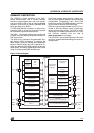
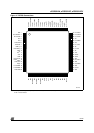
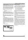
Figure 5. Memory Map and Address Space
AI07425
SECONDARY
FLASH
FLASH
MAIN
16KB
64KB
FF
7F
0
2KB
INT. RAM
EXT. RAM
Addressing
Indirect
Indirect
Direct
or
Addressing
Addressing
Direct
SFR
Internal RAM Space
(256 Bytes)
External RAM Space
(MOVX)
Flash Memory Space