


uPSD3212A, uPSD3212C, uPSD3212CV
140/163
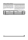
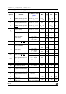
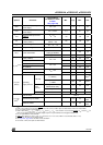
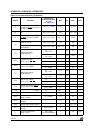
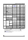
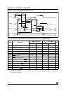
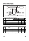
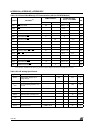
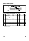
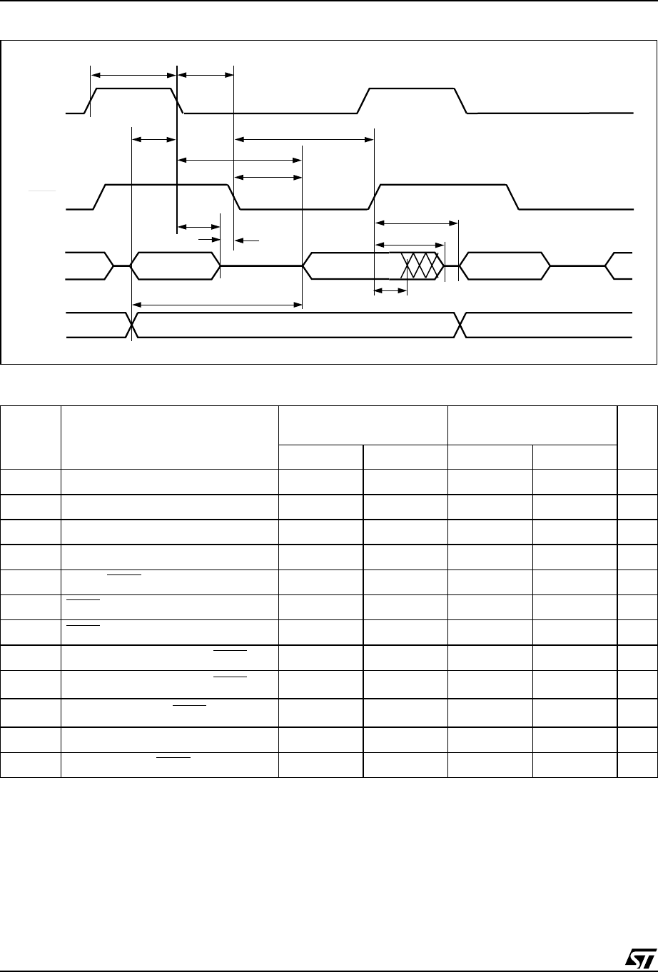
Figure 71. External Program Memory READ Cycle
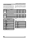
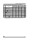
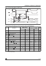
Table 116. External Program Memory AC Characteristics (with the 5V MCU Module)
Note: 1. Conditions (in addition to those in Table 109., page 133, V
CC
= 4.5 to 5.5V): V
SS
= 0V; C
L
for Port 0, ALE and PSEN output is 100pF;
C
L
for other outputs is 80pF
2. Interfacing the uPSD321x Devices to devices with float times up to 20ns is permissible. This limited bus contention does not cause
any damage to Port 0 drivers.
Symbol
Parameter
(1)
40MHz Oscillator
Variable Oscillator
1/t
CLCL
= 24 to 40MHz
Unit
Min Max Min Max
t
LHLL
ALE pulse width 35
2t
CLCL
– 15
ns
t
AVLL
Address set up to ALE 10
t
CLCL
– 15
ns
t
LLAX
Address hold after ALE 10
t
CLCL
– 15
ns
t
LLIV
ALE Low to valid instruction in 55
4t
CLCL
– 45
ns
t
LLPL
ALE to PSEN 10
t
CLCL
– 15
ns
t
PLPH
PSEN pulse width 60
3t
CLCL
– 15
ns
t
PLIV
PSEN to valid instruction in 30
3t
CLCL
– 45
ns
t
PXIX
Input instruction hold after PSEN 00ns
t
PXIZ
(2)
Input instruction float after PSEN 15
t
CLCL
– 10
ns
t
PXAV
(2)
Address valid after PSEN 20
t
CLCL
– 5
ns
t
AVIV
Address to valid instruction in 70
5t
CLCL
– 55
ns
t
AZPL
Address float to PSEN –5 –5 ns
t
AVLL
t
PLPH
t
PXIZ
t
AVIV
PSEN
PORT 2
PORT 0
AI06848
t
LHLL
ALE
t
LLPL
A0-A7
t
LLAX
t
AZPL
t
LLIV
t
PLIV
A0-A7
t
PXAV
t
PXIX
A8-A11
INSTR
IN
A8-A11