


29/163
uPSD3212A, uPSD3212C, uPSD3212CV
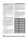
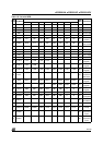
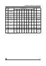
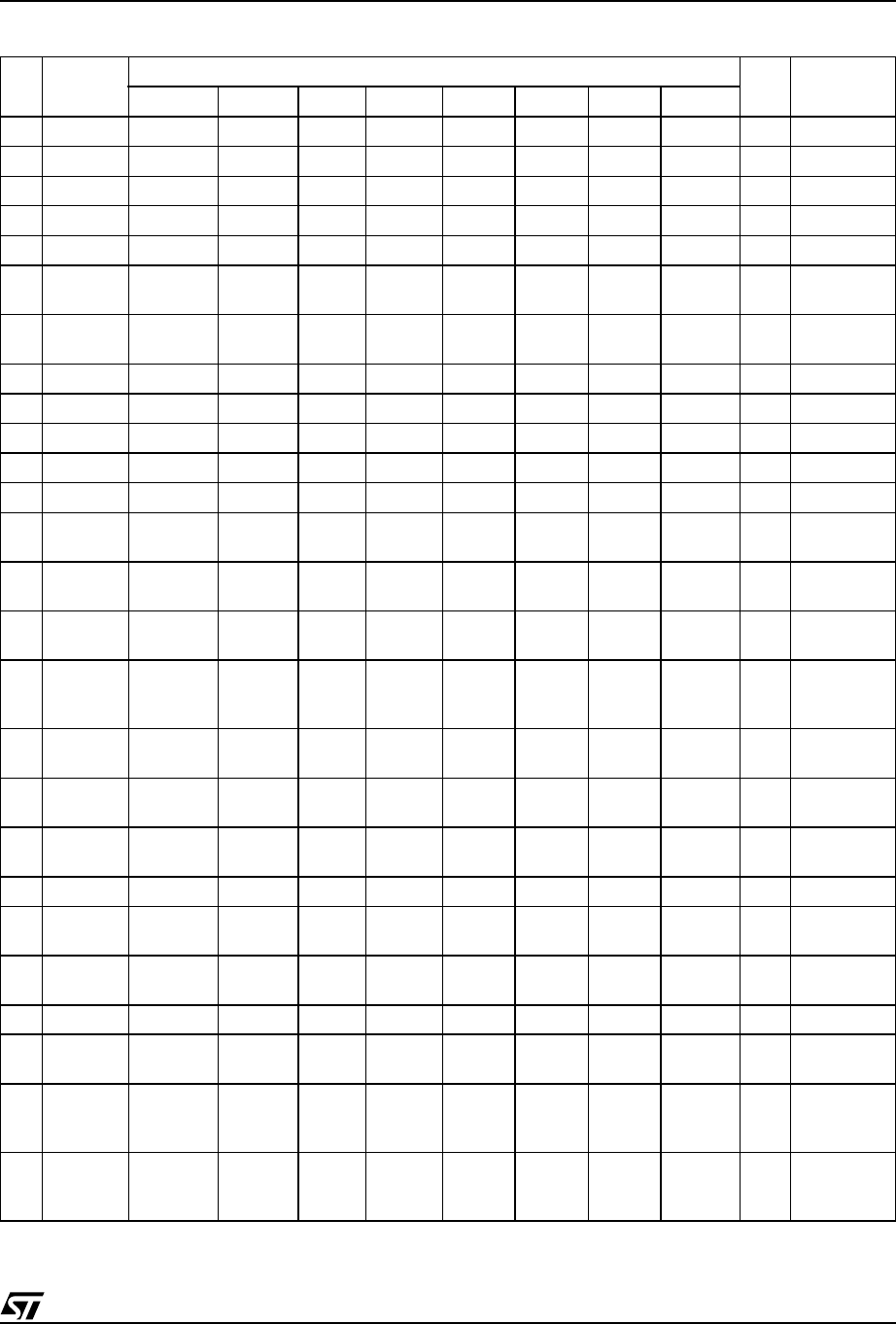
Table 16. List of all SFR
SFR
Addr
Reg Name
Bit Register Name
Reset
Value
Comments
76543210
80 P0 FF Port 0
81 SP 07 Stack Ptr
82 DPL 00 Data Ptr Low
83 DPH 00 Data Ptr High
87 PCON SMOD SMOD1 LVREN ADSFINT RCLK1 TCLK1 PD IDLE 00 Power Ctrl
88 TCON TF1 TR1 TF0 TR0 IE1 IT1 IE0 IT0 00
Timer / Cntr
Control
89 TMOD Gate C/T M1 M0 Gate C/T M1 M0 00
Timer / Cntr
Mode Control
8A TL0 00 Timer 0 Low
8B TL1 00 Timer 1 Low
8C TH0 00 Timer 0 High
8D TH1 00 Timer 1 High
90 P1 FF Port 1
91 P1SFS P1S7 P1S6 P1S5 P1S4 00
Port 1 Select
Register
93 P3SFS P3S7 P3S6 00
Port 3 Select
Register
94 P4SFS P4S7 P4S6 P4S5 P4S4 P4S3 P4S2 P4S1 P4S0 00
Port 4 Select
Register
95 ASCL 00
8-bit
Prescaler for
ADC clock
96 ADAT ADAT7 ADAT6 ADAT5 ADAT4 ADAT3 ADAT2 ADAT1 ADAT0 00
ADC Data
Register
97 ACON ADEN ADS1 ADS0 ADST ADSF 00
ADC Control
Register
98 SCON SM0 SM1 SM2 REN TB8 RB8 TI RI 00
Serial Control
Register
99 SBUF 00 Serial Buffer
9A SCON2 SM0 SM1 SM2 REN TB8 RB8 TI RI 00
2nd UART
Ctrl Register
9B SBUF2 00
2nd UART
Serial Buffer
A0 P2 FF Port 2
A1 PWMCON PWML PWMP PWME CFG4 CFG3 CFG2 CFG1 CFG0 00
PWM Control
Polarity
A2 PWM0 00
PWM0
Output Duty
Cycle
A3 PWM1 00
PWM1
Output Duty
Cycle