


149/163
uPSD3212A, uPSD3212C, uPSD3212CV
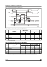
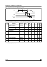
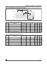
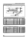
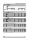
Figure 78. Input Macrocell Timing (Product Term Clock)
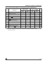
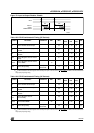
Table 129. Input Macrocell Timing (5V Devices)
Note: 1. Inputs from Port A, B, and C relative to register/ latch clock from the PLD. ALE/AS latch timings refer to t
AVLX
and t
LXAX
.
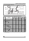
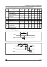
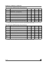
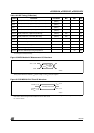
Table 130. Input Macrocell Timing (3V Devices)
Note: 1. Inputs from Port A, B, and C relative to register/latch clock from the PLD. ALE latch timings refer to t
AVLX
and t
LXAX
.
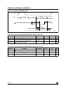
Symbol Parameter Conditions Min Max
PT
Aloc
Turbo
Off
Unit
t
IS
Input Setup Time
(Note
1)
0ns
t
IH
Input Hold Time
(Note
1)
15 + 10 ns
t
INH
NIB Input High Time
(Note
1)
9ns
t
INL
NIB Input Low Time
(Note
1)
9ns
t
INO
NIB Input to Combinatorial Delay
(Note
1)
34 + 2 + 10 ns
Symbol Parameter Conditions Min Max
PT
Aloc
Turbo
Off
Unit
t
IS
Input Setup Time
(Note
1)
0ns
t
IH
Input Hold Time
(Note
1)
25 + 20 ns
t
INH
NIB Input High Time
(Note
1)
12 ns
t
INL
NIB Input Low Time
(Note
1)
12 ns
t
INO
NIB Input to Combinatorial Delay
(Note
1)
46 + 4 + 20 ns
t
INH
t
INL
t
INO
t
IH
t
IS
PT CLOCK
INPUT
OUTPUT
AI03101