


uPSD3212A, uPSD3212C, uPSD3212CV
142/163
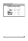
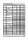
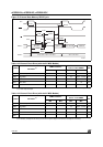
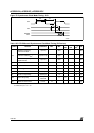
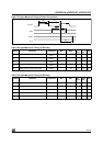
Figure 72. External Data Memory READ Cycle
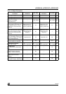
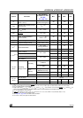
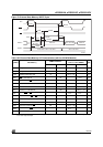
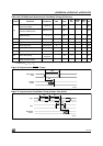
Table 118. External Clock Drive (with the 5V MCU Module)
Note: 1. Conditions (in addition to those in Table 109., page 133, V
CC
= 4.5 to 5.5V): V
SS
= 0V; C
L
for Port 0, ALE and PSEN output is 100pF;
C
L
for other outputs is 80pF
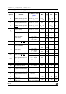
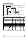
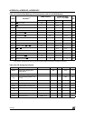
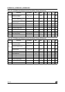
Table 119. External Clock Drive (with the 3V MCU Module)
Note: 1. Conditions (in addition to those in Table 110., page 133, V
CC
= 3.0 to 3.6V): V
SS
= 0V; C
L
for Port 0, ALE and PSEN output is 100pF,
for 5V devices, and 50pF for 3V devices; C
L
for other outputs is 80pF, for 5V devices, and 50pF for 3V devices)
Symbol
Parameter
(1)
40MHz Oscillator
Variable Oscillator
1/t
CLCL
= 24 to 40MHz
Unit
Min Max Min Max
t
RLRH
Oscillator period 25 41.7 ns
t
WLWH
High time 10
t
CLCL
– t
CLCX
ns
t
LLAX2
Low time 10
t
CLCL
– t
CLCX
ns
t
RHDX
Rise time 10 ns
t
RHDX
Fall time 10 ns
Symbol
Parameter
(1)
24MHz Oscillator
Variable Oscillator
1/t
CLCL
= 8 to 24MHz
Unit
Min Max Min Max
t
RLRH
Oscillator period 41.7 125 ns
t
WLWH
High time 12
t
CLCL
– t
CLCX
ns
t
LLAX2
Low time 12
t
CLCL
– t
CLCX
ns
t
RHDX
Rise time 12 ns
t
RHDX
Fall time 12 ns
PORT 2
PORT 0
ALE
RD
PSEN
P2.0 to P2.3 or A8-A11 from DPH A8-A11 from PCH
tAVDV
tRLDV
tLLWL
tRLRH
tAVLL
tLLDV
tLHLL
tRLAZ
DATA IN A0-A7 from PCL INSTR IN
A0-A7 from
RI or DPL
tLLAX2
tAVWL
tRHDZ
tWHLH
AI07088
tRHDX