


uPSD3212A, uPSD3212C, uPSD3212CV
32/163
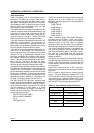
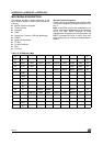
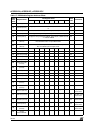
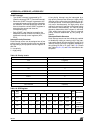
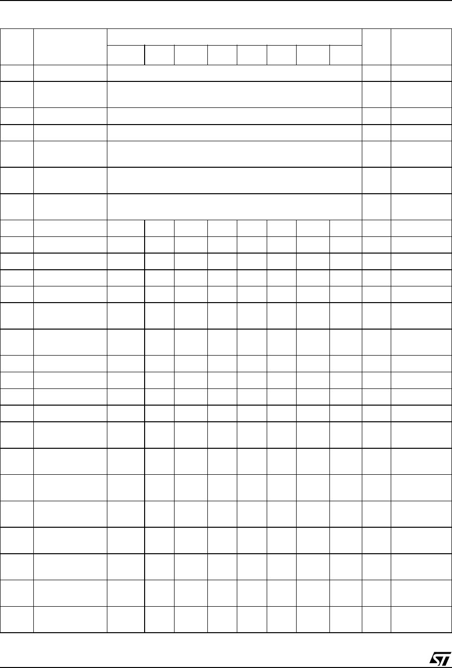
Table 17. PSD Module Register Address Offset
CSIOP
Addr
Offset
Register Name
Bit Register Name
Reset
Value
Comments
76543210
00 Data In (Port A) Reads Port pins as input
02 Control (Port A)
Configure pin between I/O or Address Out Mode. Bit = 0 selects I/
O
00
04 Data Out (Port A) Latched data for output to Port pins, I/O Output Mode 00
06 Direction (Port A) Configures Port pin as input or output. Bit = 0 selects input 00
08 Drive (Port A)
Configures Port pin between CMOS, Open Drain or Slew rate. Bit
= 0 selects CMOS
00
0A
Input Macrocell
(Port A)
Reads latched value on Input Macrocells
0C
Enable Out
(Port A)
Reads the status of the output enable control to the Port pin driver.
Bit = 0 indicates pin is in input mode.
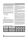
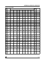
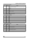
01 Data In (Port B)
03 Control (Port B) 00
05 Data Out (Port B) 00
07 Direction (Port B) 00
09 Drive (Port B) 00
0B
Input Macrocell
(Port B)
0D
Enable Out
(Port B)
10 Data In (Port C)
12 Data Out (Port C) 00
14 Direction (Port C) 00
16 Drive (Port C) 00
18
Input Macrocell
(Port C)
1A
Enable Out
(Port C)
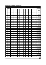
11 Data In (Port D) * * * * * *
Only Bit 1 and
2 are used
13 Data Out (Port D) * * * * * * 00
Only Bit 1 and
2 are used
15 Direction (Port D) * * * * * * 00
Only Bit 1 and
2 are used
17 Drive (Port D) * * * * * * 00
Only Bit 1 and
2 are used
1B
Enable Out
(Port D)
***** *
Only Bit 1 and
2 are used
20
Output
Macrocells AB