


101/163
uPSD3212A, uPSD3212C, uPSD3212CV
Specific Features
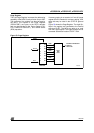
Flash Memory Sector Protect. Each primary
and secondary Flash memory sector can be sepa-
rately protected against Program and Erase cy-
cles. Sector Protection provides additional data
security because it disables all Program or Erase
cycles. This mode can be activated through the
JTAG Port or a Device Programmer.
Sector protection can be selected for each sector
using the PSDsoft Express Configuration pro-
gram. This automatically protects selected sectors
when the device is programmed through the JTAG
Port or a Device Programmer. Flash memory sec-
tors can be unprotected to allow updating of their
contents using the JTAG Port or a Device Pro-
grammer. The MCU can read (but cannot change)
the sector protection bits.
Any attempt to program or erase a protected Flash
memory sector is ignored by the device. The Verify
operation results in a READ of the protected data.
This allows a guarantee of the retention of the Pro-
tection status.
The sector protection status can be read by the
MCU through the Flash memory protection regis-
ters (in the CSIOP block). See Tables 84 and 85.
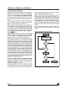
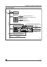
Reset Flash. The Reset Flash instruction con-
sists of one WRITE cycle (see Table
82., page 95). It can also be optionally preceded
by the standard two WRITE decoding cycles (writ-
ing AAh to 555h and 55h to AAAh). It must be ex-
ecuted after:
– Reading the Flash Protection Status or Flash
ID
– An Error condition has occurred (and the
device has set the Error Flag Bit (DQ5) to '1'
during a Flash memory Program or Erase
cycle.
The Reset Flash instruction puts the Flash memo-
ry back into normal READ Mode. If an Error condi-
tion has occurred (and the device has set the Error
Flag Bit (DQ5) to '1' the Flash memory is put back
into normal READ Mode within a few milliseconds
of the Reset Flash instruction having been issued.
The Reset Flash instruction is ignored when it is is-
sued during a Program or Bulk Erase cycle of the
Flash memory. The Reset Flash instruction aborts
any on-going Sector Erase cycle, and returns the
Flash memory to the normal READ Mode within a
few milliseconds.
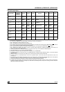
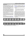
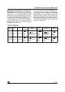
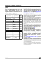
Table 84. Sector Protection/Security Bit Definition – Flash Protection Register
Note: Bit Definitions:
Sec<i>_Prot 1 = Primary Flash memory or secondary Flash memory Sector <i> is write-protected.
Sec<i>_Prot 0 = Primary Flash memory or secondary Flash memory Sector <i> is not write-protected.
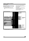
Table 85. Sector Protection/Security Bit Definition – Secondary Flash Protection Register
Note: Bit Definitions:
Sec<i>_Prot 1 = Secondary Flash memory Sector <i> is write-protected.
Sec<i>_Prot 0 = Secondary Flash memory Sector <i> is not write-protected.
Security_Bit 0 = Security Bit in device has not been set; 1 = Security Bit in device has been set.
Bit 7Bit 6Bit 5Bit 4Bit 3Bit 2Bit 1Bit 0
not used not used not used not used Sec3_Prot Sec2_Prot Sec1_Prot Sec0_Prot
Bit 7Bit 6Bit 5Bit 4Bit 3Bit 2Bit 1Bit 0
Security_Bit not used not used not used not used not used Sec1_Prot Sec0_Prot