


41/163
uPSD3212A, uPSD3212C, uPSD3212CV
The following SFR registers (Tables 29, 30, and
31) are used to control the mapping of alternate
functions onto the I/O port bits. Port 1 alternate
functions are controlled using the P1SFS register,
except for Timer 2 and the 2nd UART which are
enabled by their configuration registers. P1.0 to
P1.3 are default to GPIO after reset.
Port 3 pins 6 and 7 have been modified from the
standard 8032. These pins that were used for
READ and WRITE control signals are now GPIO
or I
2
C bus pins. The READ and WRITE pins are
assigned to dedicated pins.
Port 3 (I
2
C) and Port 4 alternate functions are con-
trolled using the P3SFS and P4SFS Special Func-
tion Selection registers. After a reset, the I/O pins
default to GPIO. The alternate function is enabled
if the corresponding bit in the PXSFS register is
set to '1.' Other Port 3 alternative functions (UART,
Interrupt, and Timer/Counter) are enabled by their
configuration register and do not require setting of
the bits in R3SFS.
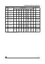
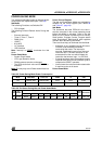
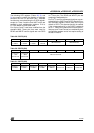
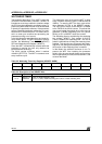
Table 29. P1SFS (91H)
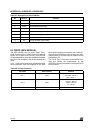
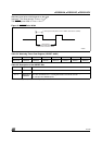
Table 30. P3SFS (93H)
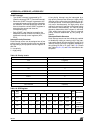
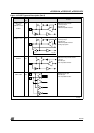
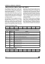
Table 31. P4SFS (94H)
76543210
0=Port 1.7
1=ACH3
0=Port 1.6
1=ACH2
0=Port 1.5
1=ACH1
0=Port 1.4
1=ACH0
Bits Reserved Bits Reserved
76543210
0 = Port 3.7
1 = SCL
from I
2
C unit
0 = Port 3.6
1 = SDA
from I
2
C unit
Bits are reserved.
76543210
0=Port 4.7
1=PWM 4
0=Port 4.6
1=PWM 3
0=Port 4.5
1=PWM 2
0=Port 4.4
1=PWM 1
0=Port 4.3
1=PWM 0
0=Port 4.2 0=Port 4.1 0=Port 4.0