


uPSD3212A, uPSD3212C, uPSD3212CV
128/163
AC/DC PARAMETERS
These tables describe the AD and DC parameters
of the uPSD321x Devices:
➜ DC Electrical Specification
➜ AC Timing Specification
■ PLD Timing
– Combinatorial Timing
– Synchronous Clock Mode
– Asynchronous Clock Mode
– Input Macrocell Timing
■ MCU Module Timing
– READ Timing
–WRITE Timing
– Power-down and RESET
Timing
The following are issues concerning the parame-
ters presented:
– In the DC specification the supply current is
given for different modes of operation.
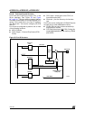
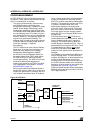
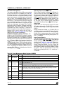
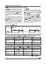
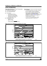
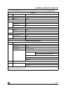
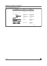
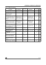
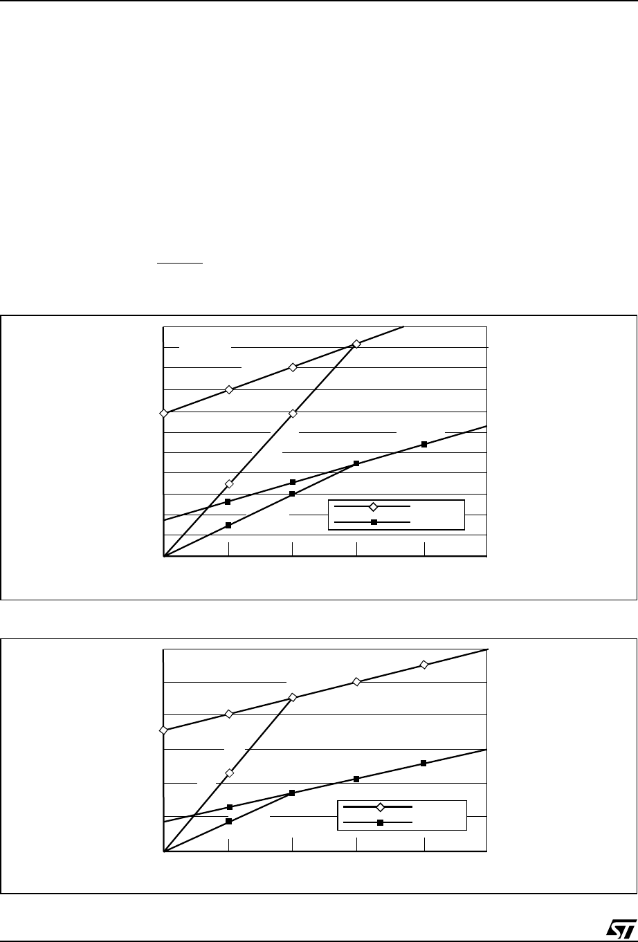
– The AC power component gives the PLD,
Flash memory, and SRAM mA/MHz
specification. Figures 68 and 69 show the PLD
mA/MHz as a function of the number of
Product Terms (PT) used.
– In the PLD timing parameters, add the
required delay when Turbo Bit is '0.'
Figure 68. PLD I
CC
/Frequency Consumption (5V range)
Figure 69. PLD I
CC
/Frequency Consumption (3V range)
0
10
20
30
40
60
70
80
90
100
110
V
CC
= 5V
50
010155 20 25
HIGHEST COMPOSITE FREQUENCY AT PLD INPUTS (MHz)
I
CC
– (mA)
TURBO ON (100%
)
TURBO ON (25%)
TURBO OFF
TURBO OFF
PT 100%
PT 25%
AI02894
0
10
20
30
40
50
60
V
CC
= 3V
010155 20 25
I
CC
– (mA)
TURBO ON (100%)
TURBO ON (25%)
TURBO OFF
TURBO OFF
HIGHEST COMPOSITE FREQUENCY AT PLD INPUTS (MHz)
PT 100%
PT 25%
AI03100