


145/163
uPSD3212A, uPSD3212C, uPSD3212CV
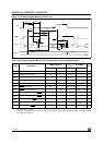
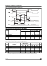
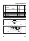
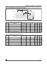
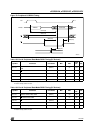
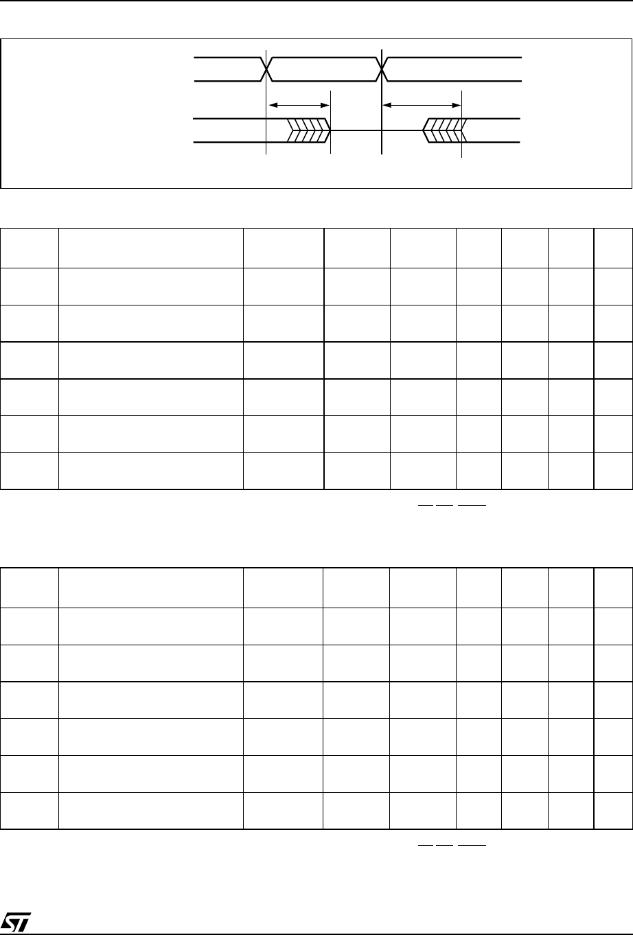
Figure 74. Input to Output Disable / Enable
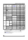
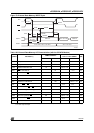
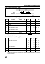
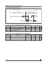
Table 123. CPLD Combinatorial Timing (5V Devices)
Note: 1. Fast Slew Rate output available on PA3-PA0, PB3-PB0, and PD2-PD1. Decrement times by given amount
2. t
PD
for MCU address and control signals refers to delay from pins on Port 0, Port 2, RD WR, PSEN and ALE to CPLD combinatorial
output (80-pin package only)
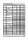
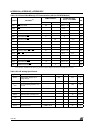
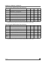
Table 124. CPLD Combinatorial Timing (3V Devices)
Note: 1. Fast Slew Rate output available on PA3-PA0, PB3-PB0, and PD2-PD1. Decrement times by given amount
2. t
PD
for MCU address and control signals refers to delay from pins on Port 0, Port 2, RD WR, PSEN and ALE to CPLD combinatorial
output (80-pin package only)
Symbol Parameter Conditions Min Max
PT
Aloc
Turbo
Off
Slew
rate
(1)
Unit
t
PD
(2)
CPLD Input Pin/Feedback to
CPLD Combinatorial Output
20 + 2 + 10 – 2 ns
t
EA
CPLD Input to CPLD Output
Enable
21 + 10 – 2 ns
t
ER
CPLD Input to CPLD Output
Disable
21 + 10 – 2 ns
t
ARP
CPLD Register Clear or Preset
Delay
21 + 10 – 2 ns
t
ARPW
CPLD Register Clear or Preset
Pulse Width
10 + 10 ns
t
ARD
CPLD Array Delay
Any
macrocell
11 + 2 ns
Symbol Parameter Conditions Min Max
PT
Aloc
Turbo
Off
Slew
rate
(1)
Unit
t
PD
(2)
CPLD Input Pin/Feedback to
CPLD Combinatorial Output
40 + 4 + 20 – 6 ns
t
EA
CPLD Input to CPLD Output
Enable
43 + 20 – 6 ns
t
ER
CPLD Input to CPLD Output
Disable
43 + 20 – 6 ns
t
ARP
CPLD Register Clear or
Preset Delay
40 + 20 – 6 ns
t
ARPW
CPLD Register Clear or
Preset Pulse Width
25 + 20 ns
t
ARD
CPLD Array Delay
Any
macrocell
25 + 4 ns
tER tEA
INPUT
INPUT TO
OUTPUT
ENABLE/DISABLE
AI02863