


uPSD3212A, uPSD3212C, uPSD3212CV
156/163
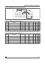
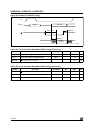
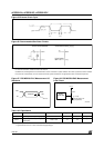
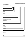
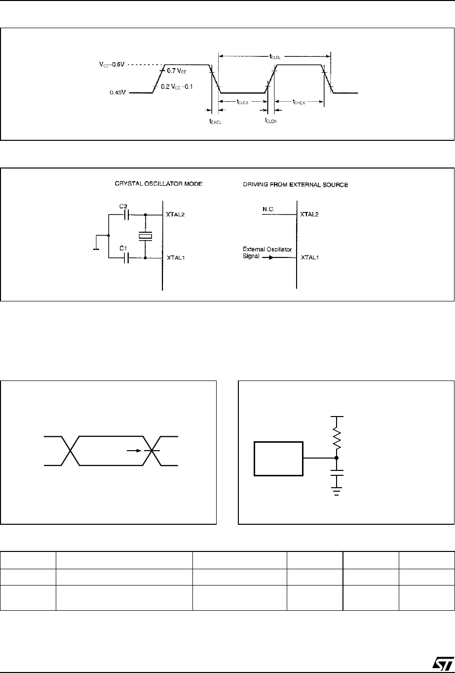
Figure 85. External Clock Cycle
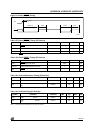
Figure 86. Recommended Oscillator Circuits
Note: C1, C2 = 30pF ± 10pF for crystals
For ceramic resonators, contact resonator manufacturer
Oscillation circuit is designed to be used either with a ceramic resonator or crystal oscillator. Since each crystal and ceramic resonator
have their own characteristics, the user should consult the crystal manufacturer for appropriate values of external components.
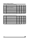
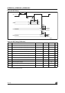
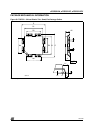
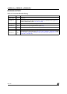
Figure 87. PSD MODULE AC Measurement I/O
Waveform
Figure 88. PSD MODULEAC Measurement
Load Circuit
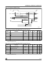
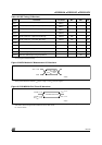
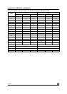
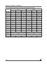
Table 143. Capacitance
Note: Sampled only, not 100% tested.
1. Typical values are for T
A
= 25°C and nominal supply voltages.
3.0V
0V
Test Point 1.5V
AI03103b
Device
Under Test
2.01 V
195 Ω
C
L
= 30 pF
(Including Scope and
Jig Capacitance)
AI03104b
Symbol Parameter Test Condition
Typ.
(1)
Max. Unit
C
IN
Input Capacitance (for input pins)
V
IN
= 0V
46
pF
C
OUT
Output Capacitance (for input/
output pins)
V
OUT
= 0V
812
pF