


uPSD3212A, uPSD3212C, uPSD3212CV
92/163
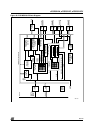
PSD MODULE REGISTER DESCRIPTION AND ADDRESS OFFSET
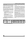
Table 81 shows the offset addresses to the PSD
MODULE registers relative to the CSIOP base ad-
dress. The CSIOP space is the 256 bytes of ad-
dress that is allocated by the user to the internal
PSD MODULE registers. Table 81 provides brief
descriptions of the registers in CSIOP space. The
following section gives a more detailed descrip-
tion.
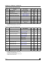
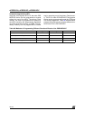
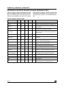
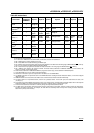
Table 81. Register Address Offset
Note: 1. Other registers that are not part of the I/O ports.
Register Name Port A Port B Port C Port D
Other
1
Description
Data In 00 01 10 11 Reads Port pin as input, MCU I/O Input Mode
Control 02 03 Selects mode between MCU I/O or Address Out
Data Out 04 05 12 13
Stores data for output to Port pins, MCU I/O
Output Mode
Direction 06 07 14 15 Configures Port pin as input or output
Drive Select 08 09 16 17
Configures Port pins as either CMOS or Open
Drain on some pins, while selecting high slew rate
on other pins.
Input Macrocell 0A 0B 18 Reads Input Macrocells
Enable Out 0C 0D 1A 1B
Reads the status of the output enable to the I/O
Port driver
Output Macrocells
AB
20 20
READ – reads output of macrocells AB
WRITE – loads macrocell flip-flops
Output Macrocells
BC
21 21
READ – reads output of macrocells BC
WRITE – loads macrocell flip-flops
Mask Macrocells AB 22 22 Blocks writing to the Output Macrocells AB
Mask Macrocells BC 23 23 Blocks writing to the Output Macrocells BC
Primary Flash
Protection
C0 Read-only – Primary Flash Sector Protection
Secondary Flash
memory Protection
C2
Read-only – PSD MODULE Security and
Secondary Flash memory Sector Protection
PMMR0 B0 Power Management Register 0
PMMR2 B4 Power Management Register 2
Page E0 Page Register
VM E2
Places PSD MODULE memory areas in Program
and/or Data space on an individual basis.