


155/163
uPSD3212A, uPSD3212C, uPSD3212CV
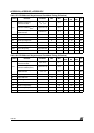
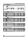
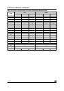
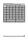
Table 142. ISC Timing (3V Devices)
Note: 1. For non-PLD Programming, Erase or in ISC By-pass Mode.
2. For Program or Erase PLD only.
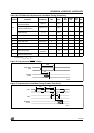
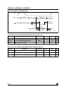
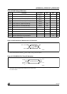
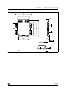
Figure 83. MCU Module AC Measurement I/O Waveform
Note: AC inputs during testing are driven at V
CC
–0.5V for a logic '1,' and 0.45V for a logic '0.'
Timing measurements are made at V
IH
(min) for a logic '1,' and V
IL
(max) for a logic '0'
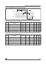
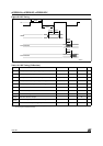
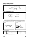
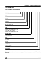
Figure 84. PSD MODULE AC Float I/O Waveform
Note: For timing purposes, a Port pin is considered to be no longer floating when a 100mV change from load voltage occurs, and begins to
float when a 100mV change from the loaded V
OH
or V
OL
level occurs
I
OL
and I
OH
≥ 20mA
Symbol Parameter Conditions Min Max Unit
t
ISCCF
Clock (TCK, PC1) Frequency (except for PLD)
(Note
1)
12 MHz
t
ISCCH
Clock (TCK, PC1) High Time (except for PLD)
(Note
1)
40 ns
t
ISCCL
Clock (TCK, PC1) Low Time (except for PLD)
(Note
1)
40 ns
t
ISCCFP
Clock (TCK, PC1) Frequency (PLD only)
(Note
2)
2MHz
t
ISCCHP
Clock (TCK, PC1) High Time (PLD only)
(Note
2)
240 ns
t
ISCCLP
Clock (TCK, PC1) Low Time (PLD only)
(Note
2)
240 ns
t
ISCPSU
ISC Port Set Up Time 12 ns
t
ISCPH
ISC Port Hold Up Time 5 ns
t
ISCPCO
ISC Port Clock to Output 30 ns
t
ISCPZV
ISC Port High-Impedance to Valid Output 30 ns
t
ISCPVZ
ISC Port Valid Output to High-Impedance 30 ns
AI06650
V
CC
– 0.5V
0.45V
Test Points
0.2 V
CC
– 0.1V
0.2 V
CC
+ 0.9V
AI06651
Test Reference Points
V
OL
+ 0.1V
V
OH
– 0.1V
V
LOAD
– 0.1V
V
LOAD
+ 0.1V
0.2 V
CC
– 0.1V