


uPSD3212A, uPSD3212C, uPSD3212CV
84/163
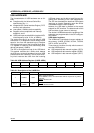
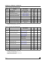
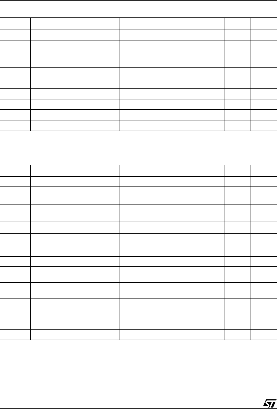
Table 78. Transceiver DC Characteristics
Note: 1. V
CC
= 5V ± 10%; V
SS
= 0V; T
A
= 0 to 70°C.
2. Level guaranteed for range of V
CC
= 4.5V to 5.5V.
3. With RPU, external idle resistor, 7.5κ±2%, D- to V
CC
.
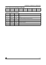
Table 79. Transceiver AC Characteristics
Note: 1. V
CC
= 5V ± 10%; V
SS
= 0V; T
A
= 0 to 70°C.
2. Level guaranteed for range of V
CC
= 4.5V to 5.5V.
3. With RPU, external idle resistor, 7.5κ±2%, D- to V
CC
.
4. C
L
of 50pF(75ns) to 350pF (300ns).
5. Measured at crossover point of differential data signals.
6. USB specification indicates 330ns.
Symb Parameter
Test Conditions
(1)
Min Max Unit
V
OH
Static Output High
15kΩ ± 5% to GND
(2,3)
2.8 3.6 V
V
OL
Static Output Low Notes 2, 3 — 0.3 V
V
DI
Differential Input Sensitivity
|(D+) - (D-)|,
Figure 43., page 86
0.2 — V
V
CM
Differential Input Common Mode Figure 43., page 86 0.8 2.5 V
V
SE
Single Ended Receiver Threshold — 0.8 2.0 V
C
IN
Transceiver Capacitance — — 20 pF
I
IO
Data Line (D+, D-) Leakage 0V < (D+,D-) < 3.3 –10 10 µA
R
PU
External Bus Pull-up Resistance, D-
7.5kΩ ± 2% to V
CC
7.35 7.65 kΩ
R
PD
External Bus Pull-down Resistance 15kΩ ± 5% 14.25 15.75 kΩ
Symb Parameter
Test Conditions
(1)
Min Max Unit
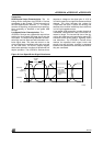
tDRATE Low Speed Data Rate Ave. bit rate (1.5Mb/s ± 1.5%) 1.4775 1.5225 Mbit/s
tDJR1 Receiver Data Jitter Tolerance
To next transition,
Figure 43., page 86
(5)
–75 75 ns
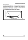
tDJR2 Differential Input Sensitivity
For paired transition,
Figure 43., page 86
(5)
–45 45 ns
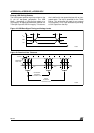
tDEOP Differential to EOP Transition Skew
Figure 44., page 87
(5)
–40 100 ns
tEOPR1 EOP Width at Receiver
Rejects as EOP
(5,6)
165 — ns
tEOPR2 EOP Width at Receiver
Accepts as EOP
(5)
675 — ns
tEOPT Source EOP Width — –1.25 1.50 µs
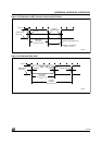
tUDJ1 Differential Driver Jitter
To next transition,
Figure 45., page 87
–95 95 ns
tUDJ2 Differential Driver Jitter
To paired transition,
Figure 45., page 87
–150 150 ns
tR USB Data Transition Rise Time Notes 2, 3, 4 75 300 ns
tF USB Data Transition Fall Time Notes 2, 3, 4 75 300 ns
tRFM Rise/Fall Time Matching
t
R
/ t
F
80 120 %
VCRS Output Signal Crossover Volt age — 1.3 2.0 V