


103/163
uPSD3212A, uPSD3212C, uPSD3212CV
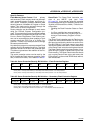
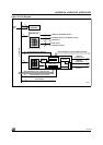
Memory Select Configuration in Program and
Data Spaces. The MCU Core has separate ad-
dress spaces for Program memory and Data
memory. Any of the memories within the PSD
MODULE can reside in either space or both spac-
es. This is controlled through manipulation of the
VM Register that resides in the CSIOP space.
The VM Register is set using PSDsoft Express to
have an initial value. It can subsequently be
changed by the MCU so that memory mapping
can be changed on-the-fly.
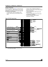
For example, you may wish to have SRAM and pri-
mary Flash memory in the Data space at Boot-up,
and secondary Flash memory in the Program
space at Boot-up, and later swap the primary and
secondary Flash memories. This is easily done
with the VM Register by using PSDsoft Express
Configuration to configure it for Boot-up and hav-
ing the MCU change it when desired. Table 86 de-
scribes the VM Register.
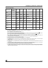
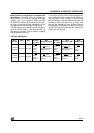
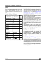
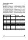
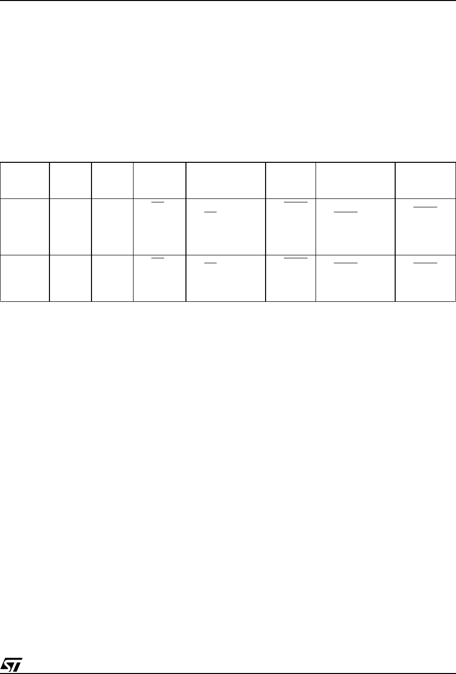
Table 86. VM Register
Bit 7
PIO_EN
Bit 6 Bit 5
Bit 4
Primary
FL_Data
Bit 3
Secondary Data
Bit 2
Primary
FL_Code
Bit 1
Secondary Code
Bit 0
SRAM_Code
0 = disable
PIO Mode
not used not used
0 = RD
can’t
access
Flash
memory
0 = RD
can’t
access Secondary
Flash memory
0 = PSEN
can’t
access
Flash
memory
0 = PSEN
can’t
access Secondary
Flash memory
0 = PSEN
can’t
access
SRAM
1= enable
PIO Mode
not used not used
1 = RD
access
Flash
memory
1 = RD
access
Secondary Flash
memory
1 = PSEN
access
Flash
memory
1 = PSEN
access
Secondary Flash
memory
1 = PSEN
access
SRAM