


115/163
uPSD3212A, uPSD3212C, uPSD3212CV
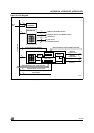
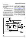
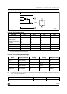
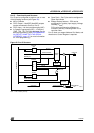
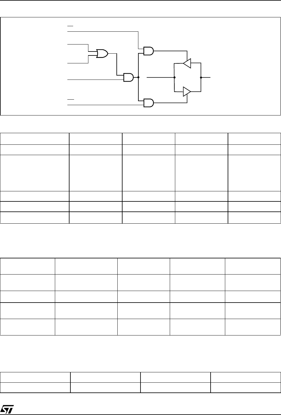
Figure 60. Peripheral I/O Mode
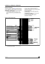
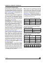
Table 89. Port Operating Modes
Note: 1. JTAG pins (TMS, TCK, TDI, TDO) are dedicated pins.
2. Port A is not available in the 52-pin package.
3. On pins PC2, PC3, PC4 and PC7 only.
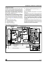
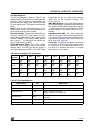
Table 90. Port Operating Mode Settings
Note: N/A = Not Applicable
Note: 1. The direction of the Port A,B,C, and D pins are controlled by the Direction Register ORed with the individual output enable product
term (.oe) from the CPLD AND Array.
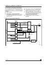
Table 91. I/O Port Latched Address Output Assignments
Port Mode
Port A
(2)
Port B Port C Port D
MCU I/O Yes Yes Yes Yes
PLD I/O
McellAB Outputs
McellBC Outputs
Additional Ext. CS Outputs
PLD Inputs
Ye s
No
No
Ye s
Yes
Yes
No
Yes
No
Ye s
(3)
No
Ye s
No
No
Ye s
Ye s
Address Out Yes (A7 – 0) Yes (A7 – 0) No No
Peripheral I/O Yes No No No
JTAG ISP No No
Ye s
(1)
No
Mode Defined in PSDsoft
Control Register
Setting
Direction Register
Setting
VM Register Setting
MCU I/O Declare pins only 0
1 = output,
0 = input (Note 1)
N/A
PLD I/O Logic equations N/A
(Note
1)
N/A
Address Out
(Port A,B)
Declare pins only 1 1 (Note 1) N/A
Peripheral I/O
(Port A)
Logic equations
(PSEL0 & 1)
N/A N/A PIO Bit = 1
Port A (PA3-PA0) Port A (PA7-PA4) Port B (PB3-PB0) Port B (PB7-PB4)
Address a3-a0 Address a7-a4 Address a3-a0 Address a7-a4
RD
PSEL0
PSEL1
PSEL
VM REGISTER BIT 7
WR
PA0-PA7
D0-D7
DATA BUS
AI02886