


113/163
uPSD3212A, uPSD3212C, uPSD3212CV
I/O PORTS (PSD MODULE)
There are four programmable I/O ports: Ports A, B,
C, and D in the PSD MODULE. Each of the ports
is eight bits except Port D, which is 3 bits. Each
port pin is individually user configurable, thus al-
lowing multiple functions per port. The ports are
configured using PSDsoft Express Configuration
or by the MCU writing to on-chip registers in the
CSIOP space. Port A is not available in the 52-pin
package.
The topics discussed in this section are:
■ General Port architecture
■ Port operating modes
■ Port Configuration Registers (PCR)
■ Port Data Registers
■ Individual Port functionality.
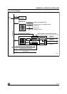
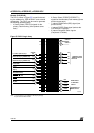
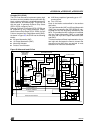
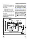
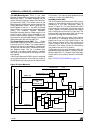
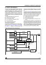
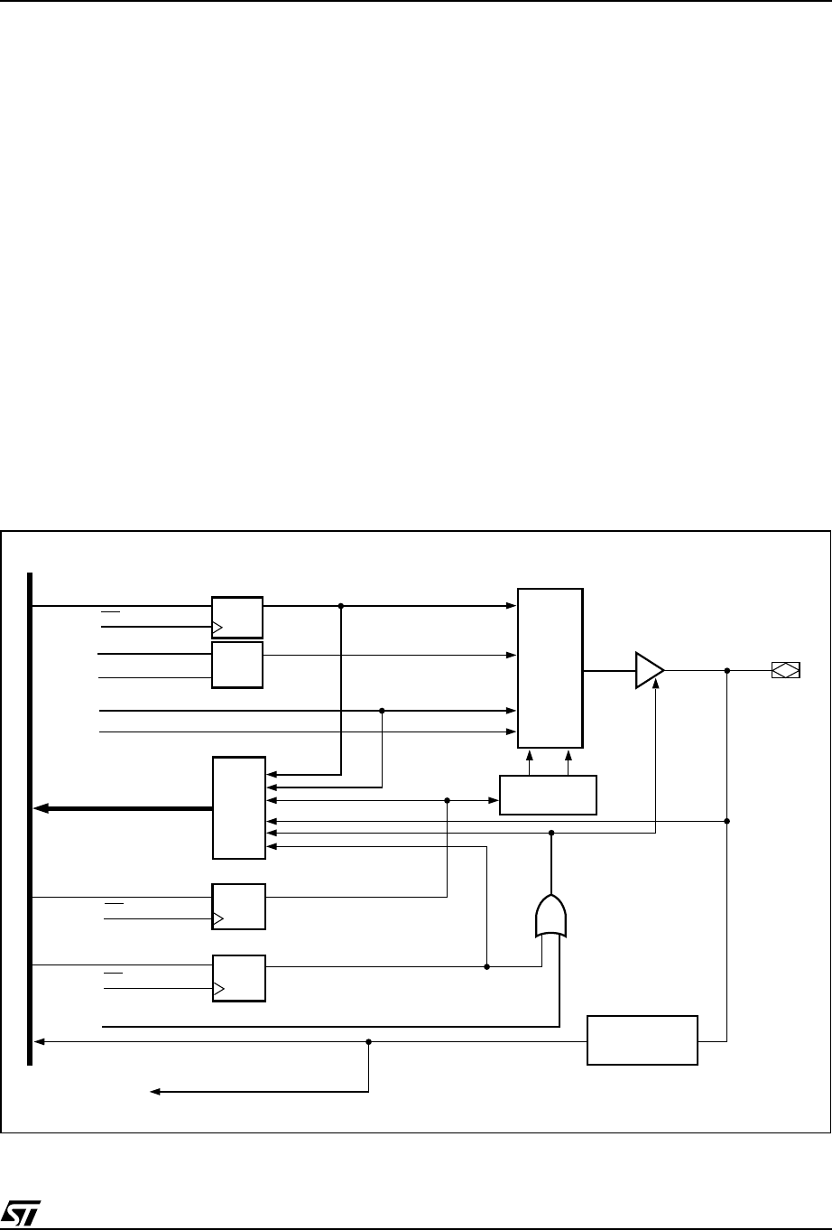
General Port Architecture
The general architecture of the I/O Port block is
shown in Figure 59. Individual Port architectures
are shown in Figure 61., page 118 to Figure
64., page 121. In general, once the purpose for a
port pin has been defined, that pin is no longer
available for other purposes. Exceptions are not-
ed.
As shown in Figure 59, the ports contain an output
multiplexer whose select signals are driven by the
configuration bits in the Control Registers (Ports A
and B only) and PSDsoft Express Configuration.
Inputs to the multiplexer include the following:
■ Output data from the Data Out register
■ Latched address outputs
■ CPLD macrocell output
■ External Chip Select (ECS1-ECS2) from the
CPLD.
The Port Data Buffer (PDB) is a tri-state buffer that
allows only one source at a time to be read. The
Port Data Buffer (PDB) is connected to the Internal
Data Bus for feedback and can be read by the
MCU. The Data Out and macrocell outputs, Direc-
tion and Control Registers, and port pin input are
all connected to the Port Data Buffer (PDB).
Figure 59. General I/O Port Architecture
MCU DATA BUS
DATA OUT
REG.
DQ
D
G
Q
DQ
DQ
WR
WR
WR
ADDRESS
MACROCELL OUTPUTS
ENABLE PRODUCT TERM
(
.OE
)
EXT CS
ALE
READ MUX
P
D
B
CPLD-INPUT
CONTROL REG.
DIR REG.
INPUT
MACROCELL
ENABLE OUT
DATA IN
OUTPUT
SELECT
OUTPUT
MUX
PORT PIN
DATA OUT
ADDRESS
AI06604