


– 21 –
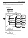
THEORY OF OPERATION
D2O
D1O
R1I
R2I
D2I
D1I
R1O
R2O
B12
B14
A15
B15
ACKDTR
R-CH
TXD
RXD
CTS
TXD0
RXD0
RXD1
CN3 CN1
IC1
CN9
IC10
IC5
Gate array
CPU
HD151232FP
B12
B14
A15
B15
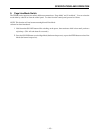
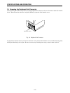
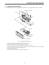
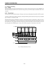
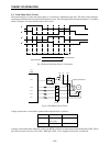
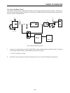
2. Main and Interface PCBs
The main PCB and interface PCB provide the drive circuitry for the TSP-400 printer series. The two boards are connected
via 40-pin connectors.
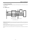
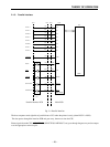
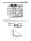
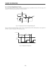
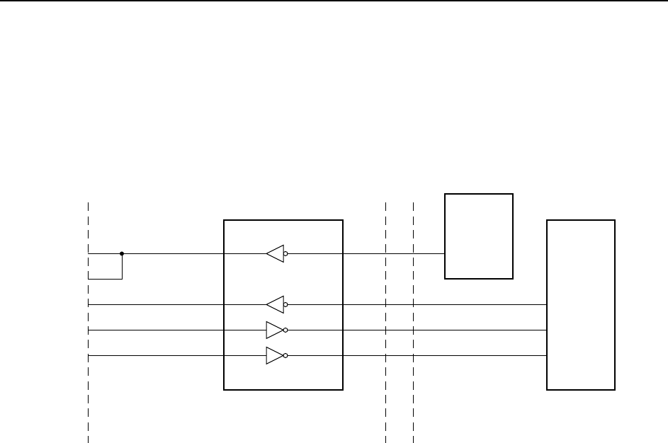
2-1. Interface
2-1-1. RS232C interface
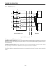
RS232C Interface PCB Main PCB
Fig. 2-2 RS232C Interface
Data flow from host to printer: IC1 receives serial data from the host computer via RXD, converts the signal voltage
from RS232C level to TTL level, and passes the result to the CPU. The CPU converts the serial data to parallel and stores
it into buffer memory.
Data flow from printer to host: The CPU generates data, converts it into serial form, then passes it to IC1. IC1 converts
the signal voltage from TTL level to RS232C level, then outputs the result over the TXD line.
The CTS line is hardware-connected, but the connection is not recognized by software. (The printer does not monitor the
signal.)