COPYRIGHT
©
2001 CANON INC. 2000 2000 2000 2000 CANON iR2200/iR2800/iR3300 REV.0 MAR. 2001
CHAPTER 1 GENERAL DESCRIPTION
1-15 S
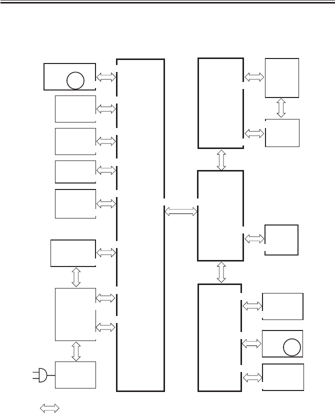
3.3 Inputs to and Outputs from the Major PCBs
3.3.1 Wiring Diagram of the Major PCBs
F01-303-01
Main
controller
PCB
DC
controller
PCB
HDD
BD
PCB
CCD PCB
Feed
PCB
Switch
PCB
Drum
sensor
PCB
Scanner
motor
Conposit
power supply
PCB
Reader
controller
PCB
J401
Laser scanner
motor
J4021
J312
J402
Laser
driver
PCB
J307/310
J301
J302
Main
power
supply
PCB
J300
J6
J111
J201
J25
J311
J1015J316
J1025
J2005
J801
J1012
J312
J403/407/408
J409
J1014
J3129
J600/601/602
LCD
panel
(LCD)
Inverter
PCB
Inverter
PCB
Control
panel
CPU PCB
J803
J3
M400
M10
J24
J3114
J1601
J136
J204
J308
J205
J500/501
J3128
Note: The in the diagram indicates connection between PCBs, NOT the flow of signals.


