


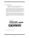
Chapter 3 Processor/Memory Subsystem
Compaq Deskpro 4000N and 4000S Personal Computers
First Edition - September 1997
3-6
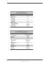
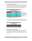
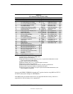
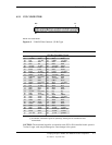
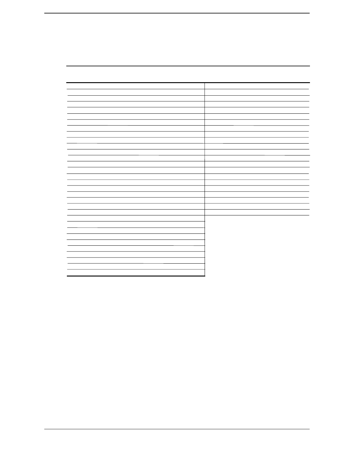
Table 3–5. SPD Address Map (SDRAM DIMM)
Table 3-5.
SPD Address Map (SDRAM DIMM)
Byte Description Notes Byte Description Notes
0 No. of Bytes Written Into EEPROM [1] 62 SPD Revision [7]
1 Total Bytes (#) In EEPROM [2] 63 Checksum Bytes 0-62
2 Memory Type 64-71 JEP-106E ID Code [8]
3 No. of Row Addresses On DIMM [3] 72 DIMM OEM Location [8]
4 No. of Column Addresses On DIMM 73-90 OEM’s Part Number [8]
5 No. of Module Banks On DIMM 91, 92 OEM’s Rev. Code [8]
6, 7 Data Width of Module 93, 94 Manufacture Date [8]
8 Voltage Interface Standard of DIMM 95-98 OEM’s Assembly S/N [8]
9 Cycletime @ Max CAS Latency (CL) [4] 99-125 OEM Specific Data [8]
10 Access From Clock [4] 126, 127 Reserved
11 Config. Type (Parity, Nonparity, etc.) 128-135 Sys. Integrator’s ID [9]
12 Refresh Rate/Type [4] [5] 136-150 Sys. Integrator’s P/N [9]
13 Width, Primary DRAM 151-152 Sys. Integrator’s D/C [9]
14 Error Checking Data Width 153-165 Sys. Integrator’s S/N [9]
15 Min. Clock Delay [6] 166 Chksm Bytes 128-165 [9]
16 Burst Lengths Supported 167-189 Top Level Sys. S/N [9]
17 No. of Banks For Each Mem. Device [4] 190-221 Avaiable for use [9]
18 CAS Latencies Supported [4] 222 Chksm Bytes 167-221 [9]
19 CS# Latency [4] 223-253 Available for use [9]
20 Write Latency [4] 254 Chksm Bytes 223-253 [9]
21 DIMM Attributes 255 Chksm Byes 0-128 [9]
22 Memory Device Attributes
23 Min. Clock Cycle Time at CL X-1 [7]
24 Max. Acc. Time From CLK at CL X-1 [7]
25 Min. Clock Cycle Time at CL X-2 [7]
26 Max. Acc. Time From CLK at CL X-2 [7]
27 Min. Row Precharge Time [7]
28 Min. Row Active To Row Active Delay [7]
29 Min. RAS to CAS Delay [7]
30, 31 Reserved
32..61 Superset Data For Future Use
NOTES:
[1] Programmed as 128 bytes by the DIMM’s OEM
[2] Must be programmed to 256 bytes.
[3] High order bit defines redundant addressing: if set (1), highest order RAS# address must be
re-sent as highest order CAS# address.
[4] Refer to memory manufacturer’s datasheet
[5] MSb is Self Refresh flag. If set (1), assembly supports self refresh.
[6] Back-to-back random column addresses.
[7] Field format proposed to JEDEC but not defined as standard at publication time.
[8] Field specified as optional by JEDEC but required by this system.
[9] Field format proposed to JEDEC. This system requires that the DIMM’s EEPROM have this
space available for reads/writes.
Access to the DIMM’s EEPROM is through an I
2
C-type bus interface using BIOS call INT 15,
AX-E827h (discussed in Chapter 8, “BIOS ROM”).
If the BIOS finds an installed module that is not supported then the memory controller is
programmed to indicate empty rows as appropriate.