


Chapter 6
MVME3100 Single Board Computer Installation and Use (6806800M28C)
105
Memory Maps
6.1 Memory Maps
6.1.1 Default Processor Memory Map
The MPC8540 presents a default processor memory map following RESET negation. The
following table shows the default memory map from the point of view of the processor. The
e500 core only provides one default TLB entry to access boot code and it allows for accesses
within the highest 4KB of memory. To access the full 8MB of default boot space (and the 1MB
of CCSR space), additional TLB entries must be set up within the e500 core for mapping these
regions. Refer to the MPC8540 Reference Manual listed in Appendix B, Related Documentation,
for details.
This is the default location for the CCSRs, but it is not mapped after reset.
Only FFFF F000 to FFFF FFFF is mapped after reset. The e500 core fetches the first instruction
from FFFF FFFC following a reset.
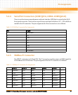
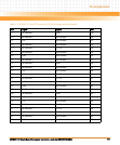
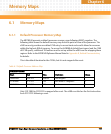
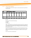
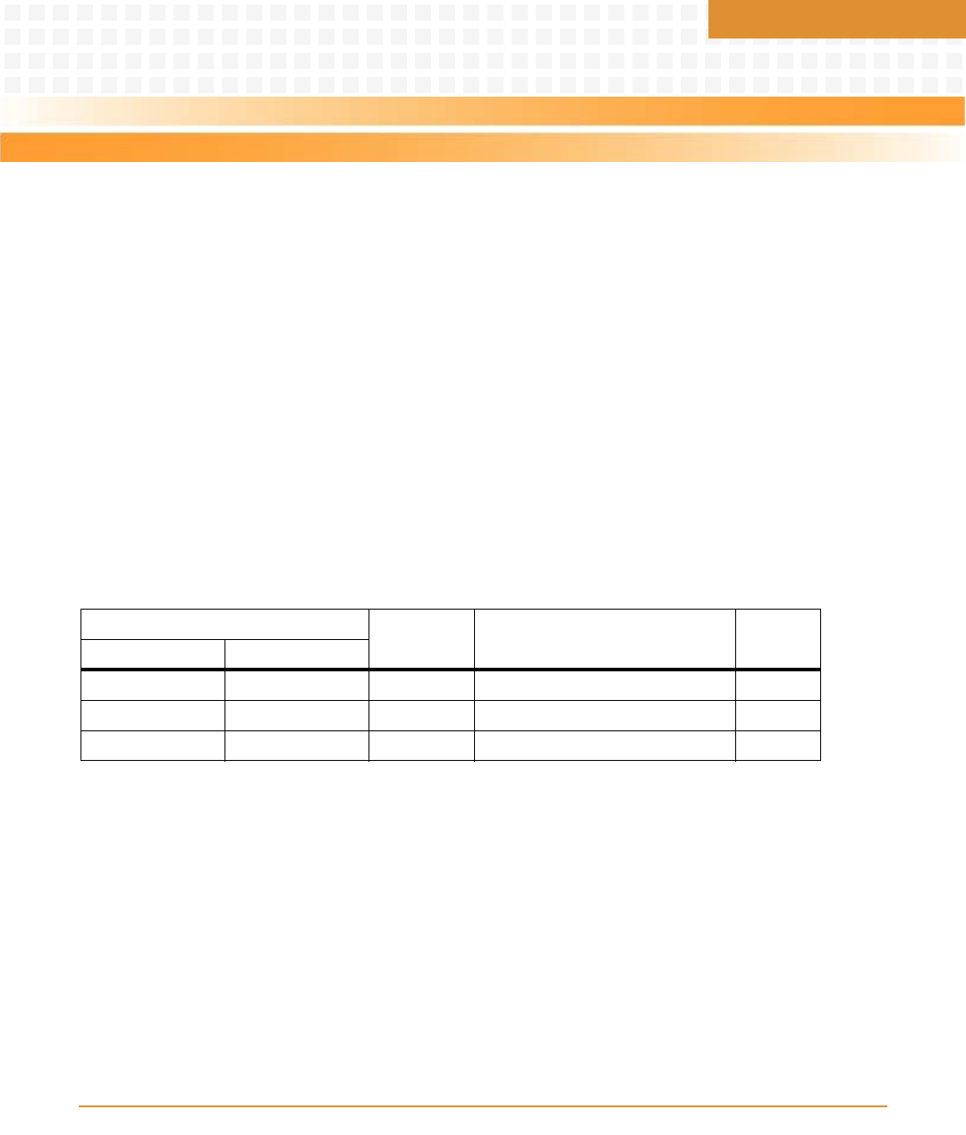
Table 6-1 Default Processor Address Map
Processor Address
Size Definition NotesStart End
0000 0000 FF6F FFFF 4087M Not mapped
FF70 0000 FF7F FFFF 1M MPC8540 CCS Registers 1
FF80 0000 FFFF FFFF 8M Flash 2