


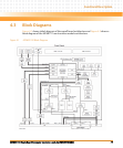

Functional Description
MVME3100 Single Board Computer Installation and Use (6806800M28C)
75
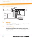
4.6 Local Bus Interface
The MVME3100 uses the MPC8540 local bus controller (LBC) for access to on-board Flash and
I/O registers. The LBC has programmable timing modes to support devices of different access
times, as well as device widths of 8, 16, and 32 bits.
The MVME3100 uses the LBC in GPCM (general purpose chip select machine) mode to
interface to two physical banks of on-board Flash, an on-board quad UART (QUART), on-board
32-bit timers, and the System Control/Status registers. Refer to the MVME3100 Single-Board
Computer Programmer’s Reference Guide listed in Appendix B, Related Documentation, for the
LBC bank and chip select assignments.
4.6.1 Flash Memory
The MVME3100 provides one physical bank of soldered-on Flash memory. The bank is
composed of two physical Flash devices configured to operate in 16-bit mode to form a 32-bit
Flash bank. The default configuration for the MVME3100-1263 is 128MB using two 512Mb
devices, and for the MVME3100-1152 it is 64MB using two 256Mb devices.
Refer to the MVME3100 Single-Board Computer Programmer’s Reference Guide listed in
Appendix B, Related Documentation, for more information.
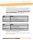
4.6.2 Control and Timers Logic
The MVME3100 control and timers logic resides on the local bus. This logic provides the
following functions on the board:
z Local bus address latch
z Chip selects for Flash banks and QUART
z System Control and Status registers
z Four 32-bit tick timers
z Real-time clock (RTC) 1 MHz reference clock
Refer to the MVME3100 Single-Board Computer Programmer’s Reference Guide listed in Appendix
B, Related Documentation, for more information.