


Memory Maps
MVME3100 Single Board Computer Installation and Use (6806800M28C)
119
6.1.15 Test Register 2
The MVME3100 provides a second 32-bit test register that reads back the complement of the
data in test register 1.
TEST2: A read from this address returns the complement of the data pattern in test register 1.
A write to this address writes the uncomplemented data to register TEST1.
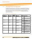
6.1.16 External Timer Registers
The MVME3100 provides a set of tick timer registers for access to the four external timers
implemented in the timers/registers PLD. These registers are 32-bit registers and are not byte
writable. The following sections describe the external timer prescaler and control registers.
6.1.16.1 Prescalar Register
The prescaler provides the clock required by each of the four timers. The tick timers require a 1
MHz clock input. The input clock to the prescaler is 25 MHz. The default value is set for $E7,
which gives a 1 MHz reference clock for a 25 MHz input clock source.
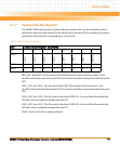
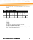
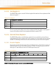
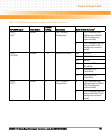
Table 6-16 Test Register 2
REG Test Register 2 - 0xE2000014
BIT 31:0
FIELD TEST2
OPER R/W
RESET FFFF
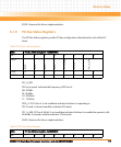
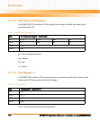
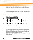
Table 6-17 Prescalar Register
REG Prescalar Register - 0xE2020000 (8 bits of 32)
BIT 76543210
FIELD Prescalar Adjust
OPER R/W
RESET $E7