


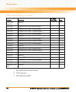
Memory Maps
MVME3100 Single Board Computer Installation and Use (6806800M28C)
112
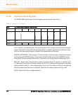
6.1.8 Flash Control/Status Register
The MVME3100 provides software-controlled bank write protect and map select functions as
well as boot block select, bank write protect, and activity status for the Flash.
FLASH_RDY: Flash ready. This bit provides the current state of the Flash devices’ Ready/Busy#
pins. These open drain output pins from each Flash device are wire OR'd to form Flash Ready.
FBT_BLK_SEL: Flash boot block select. This bit reflects the current state of the BOOT BLOCK B
SELECT switch. A cleared condition indicates that boot block A is selected and mapped to the
highest address. A set condition indicates that boot block B is selected and mapped to the
highest address.
F_WP_HW: Hardware Flash bank write protect switch status. This bit reflects the current state
of the FLASH BANK WP switch. A set condition indicates that the entire Flash bank is write
protected. A cleared condition indicates that the Flash bank is not write protected.
F_WP_SW: Software Flash bank write protect. This bit provides software-controlled
protection against inadvertent writes to the Flash memory devices. A set condition indicates
that the entire Flash is write-protected. A cleared condition indicates that the Flash bank is not
write-protected, only when the hardware write-protect bit is also not set. This bit is set during
reset and must be cleared by the system software to enable writing of the Flash devices.
MAP_SEL: Memory map select. When this bit is cleared, the Flash memory map is controlled
by the Flash Boot Block Select switch. When the map select bit is set, boot block A is selected
and mapped to the highest address.
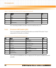
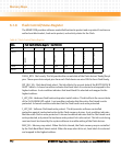
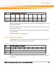
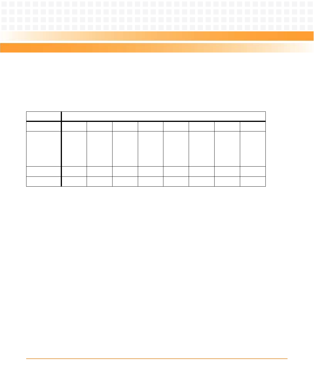
Table 6-7 Flash Control/Status Register
REG Flash Control/Status Register - 0xE2000003
BIT 76543210
FIELD
RSVD
RSVD
RSVD
MAP_SEL
F_WP_SW
F_WP_HW
FBT_BLK_SEL
FLASH_RDY
OPERRRRR/WR/WRRR
RESET00001XX1