MVME7100 Single Board Computer Installation and Use (6806800E08A)
Functional Description Block Diagram
68
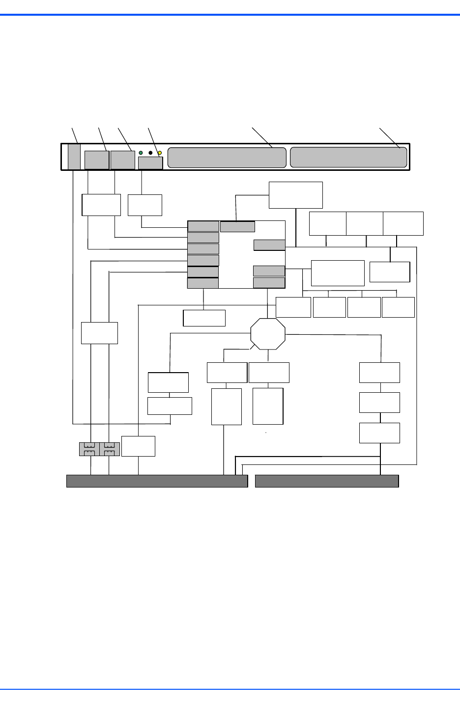
4.2 Block Diagram
The following figure is a block diagram of the MVME7100 architecture.
4.3 Processor
The MVME7100 is designed to support the MC864xD (dual e600 core) processor. The
processor is configured to operate at 1.067 GHz or 1.33 GHz core frequency with a
corresponding DDR400 Mb or DDR533 DDR2 memory bus.
Figure 4-1 Block Diagram
Flash
4 or 8 GB
Front Panel
PHY
5482
Device
Bus
GigE 1
XMCspan
P1
USB
uPD720101
QUART
16C554
PHY
5482
P2
DDR2 MC
DUART
TSEC1
TSEC2
TSEC4
LBC
PCI-E
I
2
C
CPLD
Decode
Timers/Regs
XCVR
RS-232
GigE 3
GIgE 4
Serial Ports 1-4
GigE 3
GigE 4
COM2-
COM5
PMC 1 Jn4 IO
PMC1 Front IO
PMC2 Front IO
PMC 1
PMC 2
GigE
RJ-45
TSEC3
GigE 2
VPD
8 KB
MRAM
512 KB
Flash
128 MB
PCI -E
Switch
PCI
-E
USB
GigE
RJ-45
ABT/RST
COM
VME Bus
I
2
C Bus
Serial Port 0
User
128 KB
RTC
DS1375
Up to 4 GB
DDR2 Memory
(SPD)
Temp
MAX6649
E2P
PEX8114
E2P
PEX8114
E2P
PEX8114
E2P
PEX8112
VME
Tsi148
XCVR
22501
XCVR
RS-232
I
2
C Bus
MC864xD
Processor


