


XMC Expansion Functional Description
MVME7100 Single Board Computer Installation and Use (6806800E08A)
73
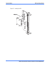
4.11 XMC Expansion
The MVME7100 provides an additional XMC/PMC module capability through the use of a 78-
pin stacking connector. This connector is connected to the second PCI Express port on the
processor. Up to four additional XMC/PMC modules may be added by using two expansion
boards. Refer to the XMCspan datasheet for additional details and/or programming information.
4.12 Power Supplies
The MVME7100 on-board voltages will be generated using Linear Tech LTC3828 dual output
two phase controllers and LTC3416 single output controllers. The following sections detail the
MVME7100 power requirements.
4.12.1 Power Sequencing
In order to meet the power sequencing requirements of the various components on the
MVME7100, the power supply controllers implement voltage tracking which allows the power
supply outputs to track each other coincidentally during power up and power down. The +3.3 V
supply output will be used as the tracking reference. All supply outputs will reach their final
values within 20 milliseconds during power up.
4.12.2 Power Supply Monitor
Logic is provided on-board to monitor the PGOOD signal from the LTC3828 and LTC3416
regulators to determine if the power supply outputs are within tolerance. If any of the power
supplies fail, this logic shuts off the power supplies to avoid any component damage. If the +5.0
V power supply is still good during a fail condition, a planar red LED (PWR FAIL D9) is
illuminated to indicate the power supply fail condition.
4.12.3 Power Supply Filtering and Fusing
Each of the switching power supply inputs on the MVME7100 will have an inductor to reduce
switching noise from being fed back onto the +5.0 V input. The LTC3828 supplies will each have
a 10 A fuse to protect the supplies from over-current in case of component failure.
4.13 Clock Distribution
The clock function generates and distributes all of the clocks required for system operation. The
PCI-E clocks are generated using an eight output differential clock driver. The PCI/PCI-X bus
clocks are generated by the bridge chips from the PCI-E clock. Additional clocks required by
individual devices are generated near the devices using individual oscillators. For clock
assignments, refer to the MVME7100 Single Board Computer Programmer’s Reference
manual.