


Theory of Operation (2620A/2625A)
Detailed Circuit Description
2
2-29
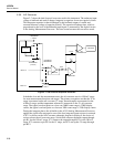
2-64. Display PCA
Display Assembly operation is classified into six functional circuit blocks: the Main
PCA Connector, the Front Panel Switches, the Display, the Beeper Drive Circuit, the
Watchdog Timer/Reset Circuit, and the Display Controller. These blocks are described
in the following paragraphs.
2-65. Main PCA Connector
The 20-pin Main PCA Connector (A2J1) provides the interface between the Main PCA
and the other functional blocks on the Display PCA. Seven of the connector pins provide
the necessary connections to the four power supply voltages (-30V dc, -5V dc, +5.1V dc,
and 5.4V ac filament voltage). Six pins are used to provide the interface to the Front
Panel Switches (A2SWR1 through A2SWR6). The other seven signals interface the
Microprocessor (A1U4) to the Display Controller (A2U1) and pass the reset signals
between the assemblies.
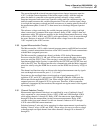
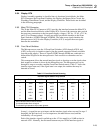
2-66. Front Panel Switches
The Microprocessor scans the 19 Front Panel Switches (A2S1 through A2S18, and
A2S21) using only six interface signals (plus the ground connection already available
from the power supply). These six signals (SWR1 through SWR6) are connected to a
bidirectional I/O port on the microprocessor. Each successive column has one less
switch.
This arrangement allows the unused interface signals to function as strobe signals when
their respective column is driven by the Microprocessor. The Microprocessor cycles
through six steps to scan the complete Front Panel Switch matrix. Table 2-7 shows the
interface signal state and, if the signal state is an output, the switches that may be
detected as closed.
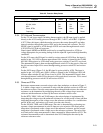
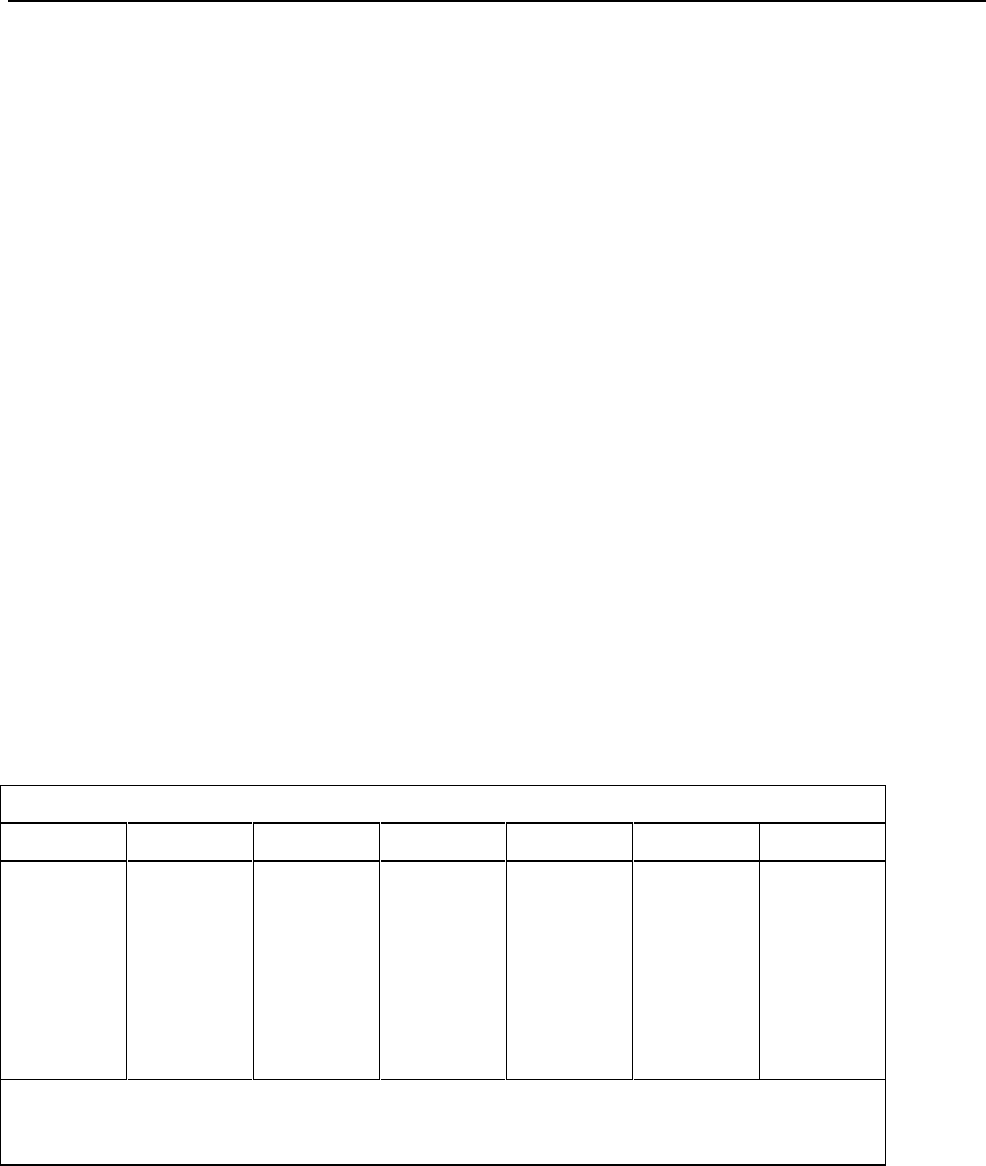
Table 2-7. Front Panel Switch Scanning
Interface Signal States or Key Sensed
Step SWR6 SWR5 SWR4 SWR3 SWR2 SWR1
1 A2S8 A2S17 A2S10 A2S12 A2S18 A2S13
2 A2S1 A2S2 A2S3 A2S4 A2S11 0
3 A2S7 A2S9 A2S5 A2S6 0 Z
4 A2S14 A2S15 A2S16 0 Z Z
5NANA0 Z Z Z
6 A2S21 0 Z Z Z Z
A2Sn indicates switch closure sensed.
0 indicated strobe driven to logic 0
Z indicated high impedance input; state ignored.
In step 1, six port bits are set to input, and the interface signal values are read. In steps 2
through 6, the bit listed as O is set to output zero, the other bits are read, and bits
indicated by a Z are ignored.
Each of the interface signals is pulled up to the +5V dc supply by a 10-kΩ resistor in
network A2Z1. Normally, the resistance between any two of the interface signals is