Theory of Operation (2620A/2625A)
Detailed Circuit Description
2
2-31
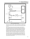
4.75-second watchdog timeout period. Each time a low-to-high transition of DISTX is
detected on A2U5-2, capacitor A2C2 is discharged to restart the timeout period. If there
are no low-to-high transitions on DISTX during the 4.75-second period, A2U5-13
transitions from high to low, triggers the other half of A2U5, and causes output A2U5-12
to go low. A2U5-12 is then inverted by A2U6 to drive the RESET signal high, causing a
system reset. The low duration of A2U5-12 is determined by timing components A2Z1
and A2C4 and is nominally 460 µs. When A2U5-12 goes high again, RESET goes low to
retrigger the Watchdog Timer.
2-70. Display Controller
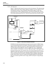
The Display Controller is a four-bit, single-chip microcomputer with high-voltage
outputs that are capable of driving a vacuum-fluorescent display directly. The controller
receives commands over a three-wire communication channel from the Microprocessor
on the Main Assembly. Each command is transferred serially to the Display Controller
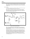
on the display transmit (DISTX) signal, with bits being clocked into the Display
Controller on the rising edges of the display clock signal (DSCLK). Responses from the
Display Controller are sent to the Microprocessor on the display receive signal (DISRX)
and are clocked out of the Display Controller on the falling edge of DSCLK.
Series resistor A2R11 isolates DSCLK from A2U1-40, preventing this output from
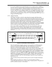
trying to drive A1U4-16 directly. Figure 2-8 shows the waveforms during a single
command byte transfer. Note that a high DISRX signal is used to hold off further
transfers until the Display Controller has processed the previously received byte of the
command.
BIT 7
BIT 7
HOLD OFF
CLEAR TO
RECEIVE
26 µs
DISTX
DSCLK
DISRX
CLEAR TO
RECEIVE
26 µs
BIT 6 BIT 5 BIT 4 BIT 3 BIT 2 BIT 1 BIT 0
BIT 6 BIT 5 BIT 4 BIT 3 BIT 2 BIT 1 BIT 0
s8f.eps
Figure 2-8. Command Byte Transfer Waveforms
Once reset, the Display Controller performs a series of self-tests, initializing display
memory and holding the DISRX signal high. After DISRX goes low, the Display
Controller is ready for communication; on the first command byte from the
Microprocessor, the Display Controller responds with a self-test results response. If all
self-tests pass, a response of 00000001 (binary) is returned. If any self-test fails, a
response of 01010101 (binary) is returned. The Display Controller initializes its display
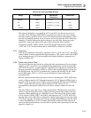
memory to one of four display patterns depending on the states of the DTEST* (A2U1-
41) and LTE* (A2U1-13) inputs. The DTEST* input is pulled up by A2Z1, but may be
pulled down by jumpering A2TP4 to A2TP3 (GND). The LTE* input is pulled down by
A2R12, but may be pulled up by jumpering A2TP5 to A2TP6 (VCC). The default
conditions of DTEST* and LTE* cause the Display Controller to turn all segments on
bright at power-up.
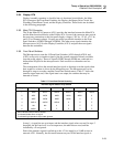
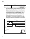
Table 2-8 defines the logic and the selection process for the four display initialization
modes.
The two display test patterns are a mixture of on and off segments forming a
recognizable pattern that allows for simple testing of display operation. Test patterns #1
and #2 are shown in Section 5 of this manual.


