


HYDRA
Service Manual
2-34
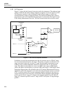
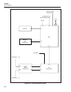
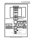
the WE* signal is low, NAND gate output A6U2-3 goes high to latch the data bus into
the lower part of the page register (A6U1).When register select PAGEH goes high and
the WE* signal is low, NAND gate output A6U2-8 goes high to latch the lower three bits
of the data bus into the high part of the page register (A6U4).
2-75. Byte Counter
The Byte Counter is a seven-bit ripple counter that controls the lower address bits of the
nonvolatile RAMs. This counter is cleared when a new value is written to the lower page
register. It automatically increments at the end of each read or write access to the
memory data register.
NAND gate output A6U2-3 goes high to write the lower page register and clear the Byte
Counter. When data is read from or written to the Non-Volatile Memory, NAND gate
output A6U2-6 goes high during the memory cycle, and then low at the end of the
memory cycle. The transition from high to low increments the Byte Counter so that the
next access to the memory data register will be for the next sequential byte in the Non-
Volatile Memory.
2-76. Nonvolatile Memory
The Non-Volatile Memory is made up of two 128K-byte static CMOS memories with
integrated lithium battery, power-fail detection, and battery switching circuitry. When
the VCC (+5.1V dc) power supply is above +4.5V dc, memories A6U6 and A6U7 are
fully operational. When VCC drops below approximately +4.25V dc, all access to the
memory are disabled by the internal power-fail detection circuit. When VCC drops
below about +3.0V dc, the battery switching circuitry disconnects VCC and connects the
lithium battery to the memory so that data is retained while the instrument power is off.
The most significant bit of the Page Register (A6U4-1,16) is gated with the MEMORY
register select signal by A6U5 to get the memory chip select signals (A6U5-6 and
A6U5-8). Memory pages 0 through 1023 are stored in memory device A6U7, and
memory pages 1024 through 2047 are stored in memory device A6U6. The WR* and
RD* control signals from the Microprocessor on the Main PCA are used to enable
writing of data to and reading data from the memory devices, respectively.
2-77. IEEE-488 Interface (Option -05)
Refer to Section 7 for detailed circuit description of this option.