


LIST OF ILLUSTRATIONS
Figure
Page No.
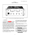
1-1 DC Power Supply, Model 6259B, 6260B, 6261B, 6268B, or 6269B . . . . . . . . . . . .. l-l
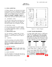
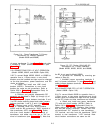
2-1 Outline Diagram . . . . . . . . . . .
. . . . . . . . . . . . . . . . . . . . . . . . . . . . . . . . . . . . . . . . . . . .
2-1
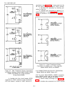
2-2 Bias Transformer Primary Connections for 208Vac and 115Vac Operation . . . . . . .2-2
2-3
Power Transformer Primary Connections for 208Vac and 115Vac Operation . . . ...2-2
2-4 Power Transformer T1 Primary Connections for 208Vac Operation. . . . . . . . . . . . .. 2-3
2-5 RF I Choke (A2L1A/A2L1B) Connections for 115Vac Operation . . . . . . . . . . . . . . ...2-3
3-1 Front Panel Controls and Indicators
. . . . . . . . . . . . . . . . . . . . . . . . . . . . . . . . . . . . . .
3-1
3-2 Normal Strapping Pattern . . . . . . . . . . . . . . . . . . . . . . . . . . . . . . . . . . . . . . . . . . . . . ...3-2
3-3 Remote Resistance Programming (Constant Voltage) . . . . . . . . . . . . . . . . . . . . . . ...3-3
3-4 Remote Voltage Programming, Unity Gain (Constant Voltage) . . . . . . . . . . . . . . ...3-3
3-5 Remote Voltage Programming, Non-Unity Gain (Constant Voltage). . . . . . . . . . ...3-4
3-6 Remote Resistance Programming (Constant Current) . . . . . . . . . . . . . . . . . . . . . . ...3-4
3-7 Remote Voltage Programming, Unity Gain (Constant Current) . . . . . . . . . . . . . . ...3-5
3-8 Remote Voltage Programming, Non-Unity Gain (Constant Current). . . . . . . . . . ...3-5
3-9 Remote Sensing. . . . . . . . . . . . . . . . . . . . . . . . . . . . . . . . . . . . . . . . . . . . . . . . . . . . . . . .
3-5
3-10 Auto-Parallel Operation, Two and Three Units . . . . . . . . . . . . . . . . . . . . . . . . . . ...3-6
3-11 Auto-Series Operation, Two and Three Units . . . . . . . . . . . . . . . . . . . . . . . . . . . . ...3-7
3-12 Auto-Tracking, Two and Three Units
. . . . . . . . . . . . . . . . . . . . . . . . . . . . . . . . . . . . . .
3-8
4-1 Overall Block Diagram . . . . . . . . . . . . . . . . . . . . . . . . . . . . . . . . . . . . . . . . . . . . . . . . ...4-1
4-2 Operating Locus of a CV/CC Power Supply
. . . . . . . . . . . . . . . . . . . . . . . . . . . . . . . .
4-2
4-3 Triac Phase Control Over AC Input Amplitude . . . . . . . . . . . . . . . . . . . . . . . . . . . ...4-3
4-4 Preregulator Control Circuit Waveforms . . . .
. . . . . . . . . . . . . . . . . . . . . . . . . . . . . . .
4-4
5-1 Differential Voltmeter Substitute Test Setup . . . . . . . . . . . . . . . . . . . . . . . . . . . . . . .
5-2
5-2 Constant Voltage Load Regulation Test Setup . . . . . . . . . . . . . . . . . . . . . . . . . . . . . .
5-3
5-3 Ripple Test Setup
. . . . . . . . . . . . . . . . . . . . . . . . . . . . . . . . . . . . . . . . . . . . . . . . . . . . . .
5-4
5-4 Noise Spike Measurement Test Setup . . . . . . . . . . . . . . . . . . . . . . . . . . . . . . . . . . ...5-5
5-5
Transient Recovery Time Test Setup . . . . . . . . . . . . . . . . . . . . . . . . . . . . . . . . . . . ...5-6
5-6 Transient Recovery Time Waveforms . . . . . . . . . . . . . . . . . . . . . . . . . . . . . . . . . . . ...5-6
5-7 Current Sampling Resistor Connections . . . . . . . . . . . . . . . . . . . . . . . . . . . . . . . . . ...5-8
5-8 Constant Current Load Regulation Test Setup . . . . . . . . . . . . . . . . . . . . . . . . . . . ...5-8
5-9 Constant Current Ripple and Noise Test Setup . . . . . . . . . . . . . . . . . . . . . . . . . . ...5-9
5-10 “ZERO ADJUST’’ Section of Main Circuit Board . . . . . . . . . . . . . . . . . . . . . . . . . . ...5-19
7-1 A2 RFI Assembly Component Location Diagram . . . . . . . . . . . . . . . . . . . . . . . . . . ...7-2
7-2 A3 Interconnection Circuit Board Assembly Component Location Diagram. . . . ...7-2
7-3 Top Front Chassis Assembly Component Location Diagram . . . . . . . . . . . . . . . . . . . . 7-3
7-4 Bottom Front Chassis Assembly Component Location Diagram . . . . . . . . . . . . . ...7-4
7-5 Bottom Rear Chassis Assembly Component Location Diagram . . . . . . . . . . . . . . ...7-5
7-6 Series Regulator Emitter Resistor Assembly Component Location Diagram . . . ...7-6
7-7 A4 Heat Sink Assembly Component Location Diagram (Top View) . . . . . . . . . . . ...7-6
7-8 A4 Heat Sink Assembly Component Location Diagram (End View) . . . . . . . . . . . ...7-7
7-9 Preregulator Control Circuit Waveforms
. . . . . . . . . . . . . . . . . . . . . . . . . . . . . . . . . . .
7-7
7-10 A1 Main Printed Circuit Board Component Location Diagram. . . . . . . . . . . . . . . ...7-8
7-11 Schematic Diagram . . . . . . . . . . . . . . . . . . . . . . . .
. . . . . . . . . . . . . . . . . . . . . . . . . . . .
Foldout
v