Chapter 5 Input/Output Interfaces
5.7.2 USB PROGRAMMING
Programming the USB interface consists of configuration, which typically occurs during POST,
and control, which occurs at runtime.
5.7.2.1 USB Configuration
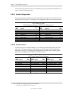
Each USB controller functions as a PCI device within the MCP component and is configured
using PCI Configuration Registers as listed in Table 5-17.
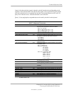
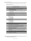
Table 5–17. USB Interface Configuration Registers
Table 5-17.
USB Interface Configuration Registers
PCI
Config.
Addr.
Register
Reset
Value
PCI
Config.
Addr.
Register
Reset
Value
00, 01h Vender ID 10DEh 0Fh BIST 00h
02, 03h Device ID [1] 10h OHCI Memory Base Addr. 0s
04, 05h PCI Command 0200h 3Ch Interrupt Line 00h
06, 07h PCI Status 00B0h 3Dh Interrupt Pin 01h
08h Revision ID A1h 3Eh Minimum Grant 03h
09h Class Code 0C0310h 3Fh Maximum Latency 01h
0Ch Cache Line Size 00h 46h Power Mgmt. Capabilities FE02h
0Dh Latency Timer 00 4Ch Specific Configuration [2]
0Eh Header Type 00h 50h USB Port Mapping [3]
NOTE:
[1] For D315 = 01C2h; for D325 = 0067h (Cntlr #1), 0067h (Cntlr #2), or 0068h (Cntlr #3)
[2] USB #1 = 02h
USB #2 = 03h
[3] The BIOS will configure this register for 2/4 operation.
5.7.2.2 USB Control
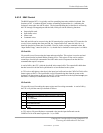
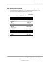
The USB is controlled through I/O registers as listed in table 5-18.
Table 5–18. USB Control Registers
Table 5-18.
USB Control Registers
I/O Addr. Register Default Value
00, 01h Command 0000h
02, 03h Status 0000h
04, 05h Interrupt Enable 0000h
06, 07 Frame Number 0000h
08, 0B Frame List Base Address 0000h
0Ch Start of Frame Modify 40h
10, 11h Port 1 Status/Control 0080h
12, 13h Port 2 Status/Control 0080h
18h Test Data 00h
5-24 Compaq D315 and hp d325 Personal Computers
Featuring the AMD Athlon XP Processor
Second Edition – April 2003


