Developer’s Manual March, 2003 10-5
Intel
®
80200 Processor based on Intel
®
XScale
™
Microarchitecture
External Bus
In addition to the alignment constraints listed above, read transactions never cross a 32-byte
boundary, and write transactions never cross a 16-byte boundary.
Some write case explanations. Byte and short writes are caused by non-cacheable non-bufferable
store commands in the Intel
®
80200 processor. The four word write can be caused by eviction of
dirty data in a cache line (the Intel
®
80200 processor has two dirty bits for each eight-word cache
line and evicts halves separately as necessary), or from the write buffer. For all writes not from
write buffer (non-cacheable writes and cache line evictions), the writes are simple and the byte
enables on the data bus are asserted for the contiguous bytes specified by the address and the length
specified in the request.
Writes coming from write buffers can look somewhat different. Due to coalescing in the write
buffers, it is possible to get a single write request on the bus writing out a non-contiguous byte
pattern. The write buffers temporarily hold outgoing store data in 4-word aligned blocks, and later
stores (byte, short, or word) to same block can be merged into (or overwrite) previous data.
Once a given write buffer is next in line for access to the bus, merging to it stops, and whatever
pattern of bytes is valid in that write buffer determines the type of write transaction sent out. The
byte enables on the bus indicates which bytes within that word are valid and need to be written.
Even if only one byte is valid in the coalesce buffer, a word store goes out. The byte enables are
only asserted for the one byte, however. This means that a single byte write request to address
0x2402 can be requested in two valid ways: a non-cacheable strb instruction causes a write of Len
0x0 (byte) to A 0x2402, with only one byte enable asserted when the data is driven; whereas a
coalesce buffer drain could cause a write of Len 0x2 (word) to A 0x2400, with only one byte
enable asserted. The same applies for two byte stores.
Notice that it is possible on a 32-bit bus for a 3-4 word write transaction to go out which requires
3-4 data cycles on the bus, but during one or more of the middle data cycles no byte enables are
asserted. The first and last data cycle always has at least one byte enable valid. Even though it
seems inefficient to waste data cycles with no byte enables, on average the merging of writes in the
write buffers can be a big performance gain.
Some examples: a pair of non-cacheable bufferable byte stores to addresses 0x2401 and 0x2403
might be merged in the write buffer. On the bus, they show up as a write of length “010” (word) to
address 0x2400. When data is driven out on the data bus, however, only byte enables for bytes 1
and 3 would be asserted.
A pair of non-cacheable bufferable byte stores to addresses 0x2401 and 0x2409 could be merged in
the write buffers and require a three word write. On a 64-bit bus, there would be two data cycles.
Both data cycles have only byte enable 1 asserted. On a 32-bit bus, there would be three data
cycles. The first and third would have 1-byte enable asserted.
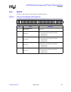
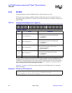
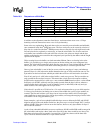
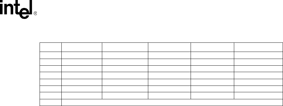
Table 10-3. Requests on a 32-bit Bus
LEN # Data Bytes # Data Bus Cycles Used for Reads? Used for Writes? Address Alignment
000 1 1 Y Y Any Address
001 2 1 Y Y A[0] = “0”
010 4 1 Y Y A[1:0] = “00”
011 8 2 N Y A[1:0] = “00”
100 12 3 N Y A[3:0] = “0X00”
101 16 4 N Y A[3:0] = “0000”
110 32 8 Y N A[1:0] = “00”
1
111 Not Used in 32-bit Bus Mode
1. On a 32-byte load, A[4:2] carries Critical Word First logic information see Section 10.2.3, “Critical Word First.


