


xii March, 2003 Developer’s Manual
Intel
®
80200 Processor based on Intel
®
XScale
™
Microarchitecture
Figures
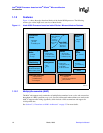
1-1 Intel
®
80200 Processor based on Intel
®
XScale
™
Microarchitecture Features ........................................... 2
3-1 Example of Locked Entries in TLB.............................................................................................................. 9
4-1 Instruction Cache Organization.................................................................................................................... 1
4-2 Locked Line Effect on Round Robin Replacement...................................................................................... 8
5-1 BTB Entry..................................................................................................................................................... 1
5-2 Branch History.............................................................................................................................................. 2
6-1 Data Cache Organization.............................................................................................................................. 2
6-2 Mini-Data Cache Organization..................................................................................................................... 3
6-3 Locked Line Effect on Round Robin Replacement.................................................................................... 15
8-1 Reset Sequence ............................................................................................................................................. 3
8-2 Pin State at Reset .......................................................................................................................................... 4
9-1 Interrupt Controller Block Diagram ............................................................................................................. 2
10-1 Typical System ............................................................................................................................................. 1
10-2 Alternate Configuration................................................................................................................................ 2
10-3 Big Endian Lane Swapping on a 64-bit Bus............................................................................................... 13
10-4 Basic Read Timing ..................................................................................................................................... 14
10-5 Read Burst, No CWF.................................................................................................................................. 15
10-6 Read Burst, CWF........................................................................................................................................ 16
10-7 Basic Word Write ....................................................................................................................................... 17
10-8 Two Word Coalesced Write ....................................................................................................................... 18
10-9 Four Word Eviction Write.......................................................................................................................... 19
10-10 Four Word Coalesced Write Burst ............................................................................................................. 20
10-11 Pipeline Example........................................................................................................................................ 21
10-12 Locked Access............................................................................................................................................ 22
10-13 Aborted Access........................................................................................................................................... 23
10-14 Hold Assertion............................................................................................................................................ 24
13-1 SELDCSR Hardware.................................................................................................................................. 18
13-2 SELDCSR Data Register............................................................................................................................ 19
13-3 DBGTX Hardware...................................................................................................................................... 21
13-4 DBGRX Hardware...................................................................................................................................... 22
13-5 RX Write Logic .......................................................................................................................................... 23
13-6 DBGRX Data Register ............................................................................................................................... 24
13-7 Message Byte Formats................................................................................................................................ 28
13-8 Indirect Branch Entry Address Byte Organization..................................................................................... 31
13-9 High Level View of Trace Buffer............................................................................................................... 32
13-10 LDIC JTAG Data Register Hardware......................................................................................................... 35
13-11 Format of LDIC Cache Functions .............................................................................................................. 37
13-12 Code Download During a Cold Reset For Debug ...................................................................................... 39
13-13 Code Download During a Warm Reset For Debug.................................................................................... 41
13-14 Downloading Code in IC During Program Execution................................................................................ 43
B-1 Intel
®
80200 Processor RISC Superpipeline................................................................................................ 3
C-1 Test Access Port Block Diagram.................................................................................................................. 2
C-2 TAP Controller State Diagram ..................................................................................................................... 7
C-3 JTAG Example ........................................................................................................................................... 13
C-4 Timing Diagram Illustrating the Loading of Instruction Register..............................................................14
C-5 Timing Diagram Illustrating the Loading of Data Register........................................................................ 15