


10-8 March, 2003 Developer’s Manual
Intel
®
80200 Processor based on Intel
®
XScale
™
Microarchitecture
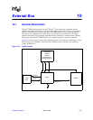
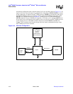
External Bus
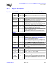
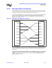
There are eight byte enables (BE#) associated with the D bus. Each byte enable corresponds to one
byte of the bus. During a write cycle, the byte enables for each byte that is being written is asserted
low. More detail on write transactions are given below.
Eight check bits, DCB, are also provided as part of the data bus. These bits are used for ECC.
Section 10.2.7, “ECC” on page 10-12, has more information on how the Intel
®
80200 processor
uses ECC.
The data bus pins D, BE#, and DCB are not driven by the Intel
®
80200 processor except when
explicitly requested by a DValid assertion for a write two clock edges earlier. This means that
when the chipset is not getting write data from the Intel
®
80200 processor it can use that bus for
other purposes or allow its use by other masters.
Between a read and a write data cycle on the data bus there should be one turnaround cycle to avoid
contention on the bus. The Intel
®
80200 processor expects this cycle and system operation is not
guaranteed without it. It is up to the chipset or SDRAM controller to control the data bus cycles.
Because the Intel
®
80200 processor transactions on the data bus must occur in the order they were
requested, DValid can be used for both read and write data cycles. Both the Intel
®
80200 processor
and the chipset have enough information to know if the Intel
®
80200 processor is driving or
sampling the data bus for any given transaction.
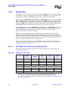
10.2.4 Configuration Pins
DBusWidth, which is on the CWF pin at reset, indicates the data bus is either 32 bits wide or
64 bits wide. If the pin is sampled as ‘0’ during reset, the Intel
®
80200 processor assumes a 64-bit
bus. If the pin is ‘1’ at reset, a 32-bit bus is assumed.