


Developer’s Manual March, 2003 C-5
Intel
®
80200 Processor based on Intel
®
XScale
™
Microarchitecture
Test Features
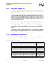
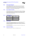
Table C-3. IEEE Instructions
Instruction /
Requisite
Opcode Description
extest
IEEE 1149.1
Required
00000
2
extest
initiates testing of external circuitry, typically board-level interconnects and
off chip circuitry.
extest connects the Boundary-Scan register between TDI and
TDO in the Shift_DR state only. When
extest is selected, all output signal pin
values are driven by values shifted into the Boundary-Scan register and may
change only on the falling-edge of TCK in the Update_DR state. Also, when
extest is selected, all system input pin states must be loaded into the
Boundary-Scan register on the rising-edge of TCK in the Capture_DR state.
Values shifted into input latches in the Boundary-Scan register are never used by
the processor’s internal logic.
sample
IEEE 1149.1
Required
00001
2
sample
/preload performs two functions:
• When the TAP controller is in the Capture-DR state, the
sample instruction
occurs on the rising edge of TCK and provides a snapshot of the
component’s normal operation without interfering with that normal operation.
The instruction causes Boundary-Scan register cells associated with outputs
to
sample the value being driven by or to the processor.
• When the TAP controller is in the Update-DR state, the
preload instruction
occurs on the falling edge of TCK. This instruction causes the transfer of data
held in the Boundary-Scan cells to the slave register cells. Typically the slave
latched data is then applied to the system outputs by means of the
extest
instruction.
dbgrx 00010
2
See Chapter 13, “Software Debug”.
clamp 00100
2
clamp
instruction allows the state of the signals driven from Intel
®
80200
processor pins to be determined from the boundary-scan register while the
Bypass register is selected as the serial path between TDI and TDO. Signals
driven from the component pins do not change while the
clamp instruction is
selected.
ldic 00111
2
See Chapter 13, “Software Debug”.
highz 01000
2
The execution of highz generates a signal that is read on the rising-edge of
RESET
. If this signal is found asserted, the device floats all its output pins. Also,
when this instruction is active, the Bypass register is connected between TDI and
TDO. This register can be accessed via the JTAG Test-Access Port throughout
the device operation. Access to the Bypass register can also be obtained with the
bypass instruction.
dcsr 01001
2
See Chapter 13, “Software Debug”.
idcode
IEEE 1149.1
Optional
11110
2
idcode
is used in conjunction with the device identification register. It connects
the identification register between TDI and TDO in the Shift_DR state. When
selected,
idcode parallel-loads the hard-wired identification code (32 bits) on
TDO into the identification register on the rising edge of TCK in the Capture_DR
state.
NOTE: The device identification register is not altered by data being shifted in on
TDI.
dbgtx 10000
2
See Chapter 13, “Software Debug”.
bypass
IEEE 1149.1
Required
11111
2
bypass
instruction selects the Bypass register between TDI and TDO pins while
in SHIFT_DR state, effectively bypassing the processor’s test logic. 0
2
is captured
in the CAPTURE_DR state. While this instruction is in effect, all other test data
registers have no effect on the operation of the system. Test data registers with
both test and system functionality perform their system functions when this
instruction is selected.