


KS152JB Universal Communications Controller
Technical Specifications
Kawasaki LSI USA, Inc. Page 71 of 120 Ver. 0.9 KS152JB2
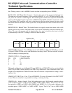
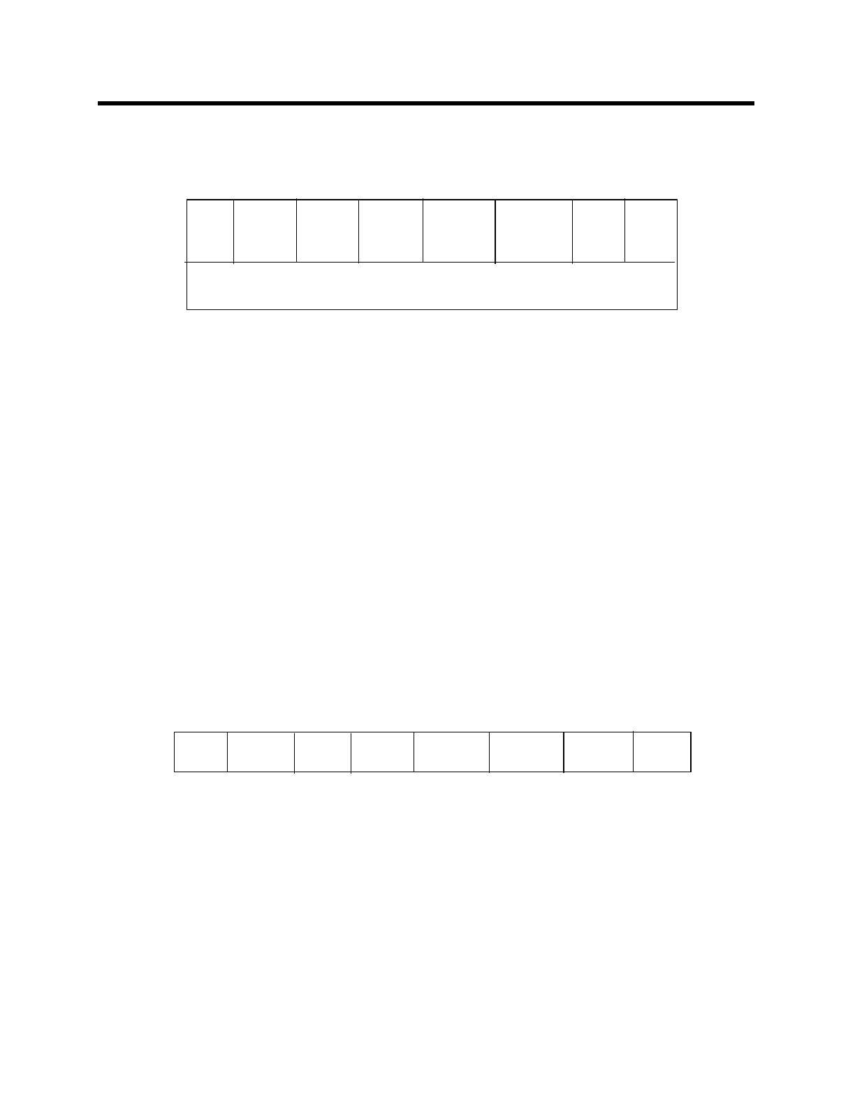
MYSLOT.0, 1,2,3,4,5 - Slot Address -The six address bits choose 1 of 64 slot addresses. Address
63 has the highest priority and address 1 has lowest. A value of zero will prevent a station from
transmitting during the collision resolution period by waiting until all the possible slot times have
elapsed. The user software normally initializes this address in the operating software.
MYSLOT.6 (DCR) - Deterministic Collision Resolution Algorithm - When set, the alternate colli-
sion resolution algorithm is selected. Retriggering of the IFS on reappearance of the carrier is also
disabled. When using this feature Alternate Backoff Mode must be selected and several other reg-
isters must be initialized. User software must initialize TCDCNT with the maximum number of
slots that are most appropriate for a particular application. The PRBS register must be set to all
ones. The disables the PRBS by freezing it’s contents at 0FFH. The backoff timer is used to count
down the number of slots based on the slot timer value setting the period of one slot. The user
software is responsible for setting or clearing this flag.
MYSLOT.7 (DCJ) - D.C.Jam - When set selects D.C. type jam, when clear, selects A.C. type jam.
The user software is responsible for setting or clearing this flag.
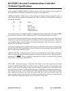
PCON contains bits for power control, LSC control, DMA control, and GSC control. The bit used
for the GSC are PCON.2, PCON.3, and PCON.4.
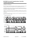
PCON.2 (GFIEN) - GSC Flag Idle Enable -Setting GFIEN to a 1 caused idle flags to be generated
between transmitted frames in SDLC mode. SDLC idle flags consists of 01111110 flags creating
the sequence 01111110011111110..........011111110. A possible side effect of enabling GFIEN is
that the maximum possible latency from writing to TFIFO until the first bit is transmitted
increased from approximately 2 bit-times to around 8 bit-times. GFIEN has not effect with
CSMA/CD.
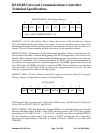
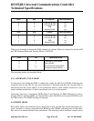
7
6
5
4
3
2
1
0
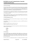
DCJ
DCR
SA5
SA4
SA3
SA2
SA1 SA0
SAn = SLOT ADDRESS (BITS 5 - 0)
MYSLOT (0F5H) - Slot Address Register
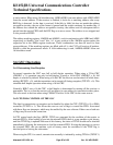
SMOD ARB
REQ
GAREN
XRCLK GFIEN PD IDL
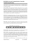
7
6
5
43
2
1
0
PCON (087H)