


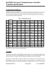
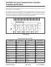
KS152JB Universal Communications Controller
Technical Specifications
Kawasaki LSI USA, Inc. Page 9 of 120 Ver. 0.9 KS152JB2
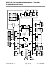
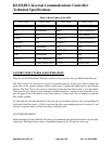
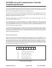
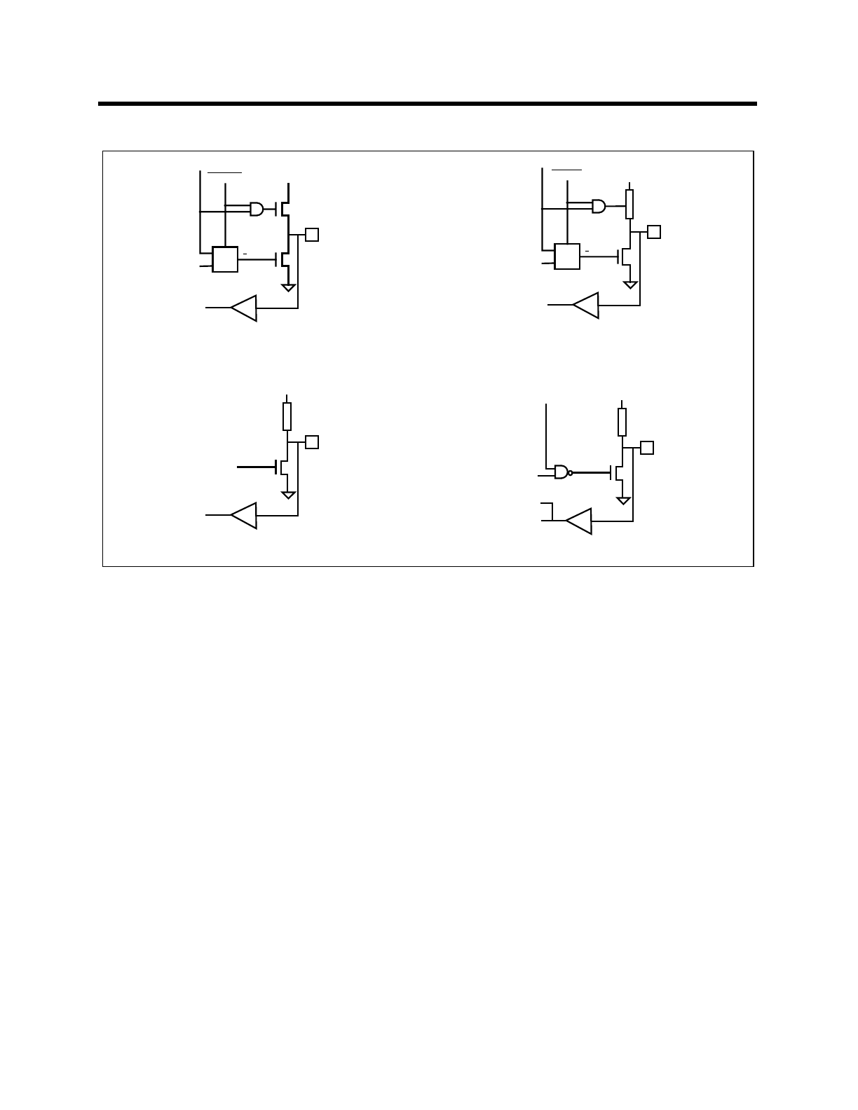
As shown in Figure above, Ports 0 and 2 can emit either their respective SFR contents or the
ADDR/DATA and ADDRESS bus, depending upon the control lines IDNAMX and IDNAHI.
During external memory accesses, the P2 SFR remains unchanged, but the P0 SFR is preset to
FFh.
Ports 1, 2, 4, 5 and 6 have internal pullups, while Port 0 has an open drain output.
Every single I/O line can be individually configured as an input or output. However Ports 0 and 2
cannot be used as I/O ports since they are used as the ADDRESS/ DATA bus. To use any port pin
as an input, the corresponding bit latch must contain a 1. This turns off the active pulldown FET.
Then, for Ports 1, 2 and 3, the pin is pulled high by the internal pullup. The Internal pullup is a
weak pullup and so the pin can be pulled low by a strong external source.
Port 0, however has no internal pullups. The active pullup FET is used only when the port pin is
emitting a 1 during external memory accesses, else the pullup is off. Hence, when the port is used
as an I/O pin; IDNAMX is 1; the pullup FET is always off. Writing a 1 to the bit latch will turn off
the active pulldown FET and as a result the port pin will float.
As port 1, 2 and 3 have internal pullups, they will go high when configured as inputs and will
source current. Hence they are also known as “quasi-bidirectional” ports. Port 0 on the other hand
“floats” when configured as an input and hence is called a “true bidirectional” port.
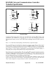
VCC
IDNAHI
ADDRESS
PORT2OP
MUX
0
1
Q
P2.X
Pin
PORT2IP
3. Port 2 I/O Pad
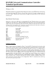
VCC
IDNAMX
ADDR/DATA
PORT0OP
MUX
0
1
Q
P0.X
Pin
PORT0IP
1. Port 0 I/O Pad
Internal
Pullup
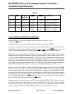
VCC
PORT1OP
P1.X
Pin
PORT1IP
2. Port 1 I/O Pad
Weak Internal
Pullup
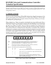
VCC
PORT3OP
P3.X
Pin
PORT3IP
4. Port 3,4,5 &6 I/O Pad
Weak Internal
Pullup
Alternate Output
Function
Alternate Output
Function
Port bit I/O Pads