


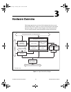

Chapter 3 Hardware Overview
PCI-4451/4452 User Manual 3-4
©
National Instruments Corporation
All data read from the ADC is interpreted as two’s complement format. In
two’s complement mode, digital data values read from the analog input
channel are either positive or negative.
Considerations for Selecting Input Ranges
The input range you select depends on the expected range of the incoming
signal. A large input range can accommodate a large signal variation but
reduces the voltage resolution. Choosing a smaller input range improves
the voltage resolution but can result in the input signal going out of range.
For best results, match the input range as closely as possible to the expected
range of the input signal.
If the input range is not appropriately chosen, an input signal can be clipped
and introduce large errors that are easily identified in the frequency
spectrum. The PCI-4451/4452 is equipped with overrange detection
circuits in both the analog and digital sections of each input channel. These
circuits determine if an input signal has exceeded the selected input
voltage. Chapter 6, Theory of Analog Operation, provides a more in-depth
explanation of how overranges can occur.
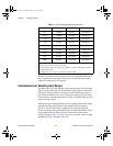
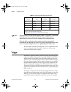
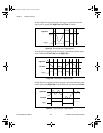
Table 3-1.
Actual Range and Measurement Precision
Linear Gain Gain Input Range Precision
1
0.1 –20 dB ±42.4 V
2
3.0518 mV
2
0.316 –10 dB ±31.6 V 965.05 µV
1.0 0 dB ±10.0 V 305.18 µV
3.16 10 dB ±3.16 V 96.505 µV
10 20 dB ±1.00 V 30.518 µV
31.6 30 dB ±0.316 V 9.6505 µV
100 40 dB ±0.100 V 3.0518 µV
316 50 dB ±31.6 mV 965.05 nV
1000 60 dB ±10.0 mV 305.18 nV
1
The value of 1 LSB of the 16-bit ADC; that is, the voltage increment corresponding to a
change of one count in the ADC 16-bit count.
2
The actual input range is by design ±100 V; however, the device is not tested or certified
to operate in this range.
See Appendix A,
Specifications
, for absolute maximum ratings.
User.book Page 4 Tuesday, April 14, 1998 10:20 AM