


Chapter 3 Hardware Overview
©
National Instruments Corporation 3-11 PCI-4451/4452 User Manual
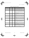
Timing Signal Routing
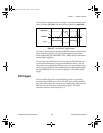
The DAQ-STC provides a flexible interface for connecting timing signals
to other devices or to external circuitry. Your PCI-4451/4452 device uses
the RTSI bus to interconnect timing signals between devices, and uses the
PFI pins on the I/O connector to connect the device to external circuitry.
These connections enable the PCI-4451/4452 device to both control and be
controlled by other devices and circuits.
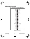
There are a total of 13 timing signals internal to the DAQ-STC that you can
control by an external source. You can also control these timing signals by
signals generated internally to the DAQ-STC, and these selections are fully
software configurable. Many of these timing signals are also available as
outputs on the RTSI pins, as indicated in the RTSI Triggers section earlier
in this chapter, and on the PFI pins, as indicated in Chapter 4, Signal
Connections.
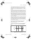
Programmable Function Inputs
The 10 PFIs are connected to the signal routing multiplexer for each timing
signal, and software can select one of the PFIs as the external source for a
given timing signal. It is important to note that you can use any of the PFIs
as an input by any of the timing signals and that multiple timing signals can
use the same PFI simultaneously. This flexible routing scheme reduces the
need to change physical connections to the I/O connector for different
applications. You can also individually enable each of the PFI pins to
output a specific internal timing signal. For example, if you need the
GPCTR0_SOURCE signal as an output on the I/O connector, software can
turn on the output driver for the PFI8/GPCTR0_SOURCE pin.
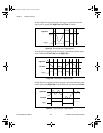
Note
Two of the 10 PFI pins are not available for general-purpose input on the digital
connector. You can configure PFI2/CONVERT* and PFI5/UPDATE* as outputs
only.
Device and RTSI Clocks
Some PCI-4451/4452 device functions require a frequency timebase to
generate the necessary timing signals for controlling general-purpose
signals at the 50-pin digital I/O connector. You cannot use these signals for
the generating the frequency of sample rates or update rates. Refer to
Selecting Sample/Update Clock Frequency section for information on
sample/update clock generation.
User.book Page 11 Tuesday, April 14, 1998 10:20 AM