


Chapter 4 Signal Connections
©
National Instruments Corporation 4-23 PCI-4451/4452 User Manual
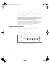
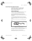
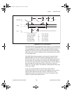
Figure 4-13.
GPCTR Timing Summary
The GATE and OUT signal transitions shown in Figure 4-13 are referenced
to the rising edge of the SOURCE signal. This timing diagram assumes that
you programmed the counters to count rising edges. The same timing
diagram, but with the source signal inverted and referenced to the falling
edge of the source signal, would apply when you programmed the counter
to count falling edges.
The GATE input timing parameters are referenced to the signal at the
SOURCE input or to one of the internally generated signals on your
PCI-4451/4452 device. Figure 4-13 shows the GATE signal referenced to
the rising edge of a source signal. The gate must be valid (either high or
low) for at least 10 ns before the rising or falling edge of a source signal for
the gate to take effect at that source edge, as shown by t
gsu
and t
gh
in
Figure 4-13. The gate signal is not required to be held after the active edge
of the source signal.
If you use an internal timebase clock, the gate signal cannot be
synchronized with the clock. In this case, gates applied close to a source
edge take effect either on that source edge or on the next one. This
arrangement results in an uncertainty of one source clock period with
respect to unsynchronized gating sources.
SOURCE
V
IH
V
IL
V
IH
V
IL
t
sc
t
sp
t
gsu
t
gh
t
gw
GATE
t
out
OUT
V
OH
V
OL
sc
t
t
t
t
t
t 50 ns minimum
sp
23 ns minimum
gsu
10 ns minimum
gh
0 ns minimum
gw
10 ns minimum
out
80 ns maximum
Source Clock Period
Source Pulse Width
Gate Setup Time
Gate Hold Time
Gate Pulse Width
Output Delay Time
t
sp
User.book Page 23 Tuesday, April 14, 1998 10:20 AM