


Section Five Programming the GPIB-COM
© National Instruments Corporation 5-3 GPIB-COM User Manual
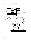
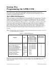
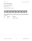
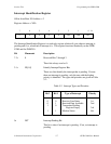
Receive Buffer Register
Offset from Base I/O Address = 0
Register Address = XF8
DLAB bit in Line Control Register = 0
7 654 321
0
D6 D5
D7
D4
D3
D2 D1 D0
R
The Receive Buffer Register contains the character received from the serial input, with bit 0 being
the least significant and bit 7 the most significant. It functions identically on the GPIB-COM and
the INS8250.
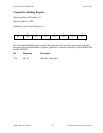
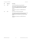
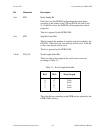
Bit Mnemonic Description
7-0r D[7-0] Data Bits 7 through 0