


Programming the GPIB-COM Section Five
GPIB-COM User Manual 5-8 © National Instruments Corporation
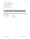
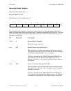
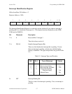
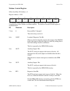
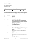
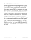
Line Control Register
Offset from Base I/O Address = 3
Register Address = XFB
7 654 321
0
SBRK STPDLAB EVEN
PEN
STB WL1 WL0 R/W
The Line Control Register is a read/write register that allows the programmer to set the RS-232
parameters for the INS8250. The function of each bit in this register is explained below.
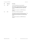
Bit Mnemonic Description
7r/w DLAB Divisor Latch Access Bit
This bit controls which registers will respond to I/O addresses
XF8 and XF9. This bit is set to access the Divisor Latch LSB
and MSB, and cleared to access the Transmitter Holding
Register, the Receive Buffer Register, and the Interrupt Enable
Register.
This bit functions identically on the GPIB-COM and the
INS8250.
6r/w SBRK Set Break Control Bit
When set, this bit causes the SOUT line of the serial cable to be
forced to a logical 0 state.
This bit is ignored by the GPIB-COM.
5r/w STP Stick Parity Bit
When this bit is set, the parity bit transmitted and detected will
be the inverse of the EVEN bit (bit 4), regardless of the number
of 1's in the data word.
This bit is ignored by the GPIB-COM.
4r/w EVEN Even Parity Select Bit
If this bit is set, even parity will be generated and checked. If
this bit is clear, odd parity will be generated and checked.
This bit is ignored by the GPIB-COM.