


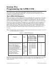

Section Five Programming the GPIB-COM
© National Instruments Corporation 5-5 GPIB-COM User Manual
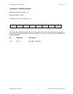
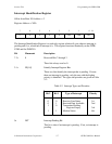
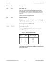
Interrupt Enable Register
Offset from Base I/O Address = 1
Register Address = XF9
DLAB bit in Line Control Register = 0
7 654 321
0
00
0
0
MS
RLS THR RDA
R/W
The Interrupt Enable Register is a read/write register that allows the programmer to selectively
enable or disable each of the four possible types of interrupts generated by the INS8250. The high
four bits are not used and are permanently cleared. The lower four bits each enable one type of
interrupt as listed below.
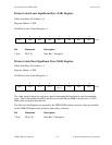
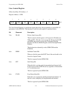
Bit Mnemonic Description
7-4r/w 0 Reserved Bits 7 through 4
These bits always read as 0.
3r/w MS Modem Status Interrupt Enable Bit
This bit enables a modem status interrupt when set to logical 1.
The modem status interrupt occurs when any of bits 0 through 3
of the Modem Status Register are set to logical 1.
This bit is identical on the GPIB-COM and the INS8250, but
bits 0 through 3 of the Modem Status Register are set for
different conditions as noted under the Modem Status Register
description.
2r/w RLS Receive Line Status Interrupt Enable Bit
This bit enables a line status interrupt when set. The line status
interrupt occurs when any of bits 1 through 4 of the Line Status
Register become set.
This bit is identical on the GPIB-COM and the INS8250, but
bits 1 through 4 of the Line Status Register are set for different
conditions as noted under the Line Status Register description.