


Programming the GPIB-COM Section Five
GPIB-COM User Manual 5-4 © National Instruments Corporation
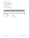
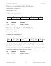
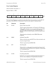
Divisor Latch Least Significant Byte (LSB) Register
Offset from Base I/O Address = 0
Register Address = XF8
DLAB bit in Line Control Register = 1
7 654 321
0
DL6 DL5
DL7
DL4
DL3
DL2 DL1 DL0 R/W
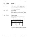
Bit Mnemonic Description
7-0r/w DL[7-0] Data Bits 7 through 0
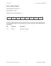
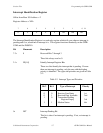
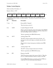
Divisor Latch Most Significant Byte (MSB) Register
Offset from Base I/O Address = 1
Register Address = XF9
DLAB bit in Line Control Register = 1
7 654 321
0
DL14 DL13
DL15
DL12
DL11
DL10 DL9 DL8 R/W
The value stored in these two registers is used to determine the baud rate for serial communica-
tions. The 16-bit number formed by the Divisor Latch LSB and MSB is divided into a 1.8432
MHz clock to produce the baud rate.
The Divisor Latch Registers are ignored by the GPIB-COM circuitry; however, they are available
on the GPIB-COM and can be written to and read by software.
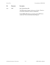
Bit Mnemonic Description
7-0r/w DL[15-8] Data Bits 15 through 8