


Programming the GPIB-COM Section Five
GPIB-COM User Manual 5-10 © National Instruments Corporation
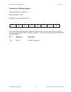
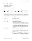
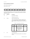
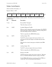
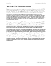
Modem Control Register
Offset from Base I/O Address = 4
Register Address = XFC
7 654 321
0
00
0
LOOP
OUT2
OUT1 RTS DTR
R/W
The Modem Control Register is a read/write register that controls RS-232 output lines for
communication with a modem or modem emulator. The function of each bit in this register is
explained below.
Bit Mnemonic Description
7-5r/w 0 Reserved Bits 7 through 5
These bits always read as 0.
4r/w LOOP Loopback Diagnostic Test Bit
When set, this bit internally connects the outputs of the INS8250
back to the inputs to allow the chip to be tested by writing data to
itself and reading it back for verification.
This bit is ignored by the GPIB-COM circuitry.
3r/w OUT2 Auxiliary Output 2 Bit
The OUT2 serial port output is the inverse of this bit. All
interrupts from the serial adapter are disabled when this bit is
cleared.
When this bit is cleared, interrupts are disabled on the GPIB-
COM.
2r/w OUT1 Auxiliary Output 1 Bit
The OUT1 serial port output is the inverse of this bit.
This bit is ignored by the GPIB-COM circuitry.
1r/w RTS Request to Send Bit
The RTS serial port output is the inverse of this bit. When this
bit is set, it indicates that the Controller is ready to send data.
On the GPIB-COM, this bit is used along with the DTR bit to
control the CTS bit of the Modem Status Register.